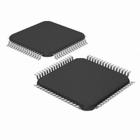
DSPIC33FJ32GS406-I/PT Microchip Technology, DSPIC33FJ32GS406-I/PT Datasheet - Page 109

DSPIC33FJ32GS406-I/PT
Manufacturer Part Number
DSPIC33FJ32GS406-I/PT
Description
IC MCU/DSP 32KB FLASH 64TQFP
Manufacturer
Microchip Technology
Series
dsPIC™ 33Fr
Specifications of DSPIC33FJ32GS406-I/PT
Core Processor
dsPIC
Core Size
16-Bit
Speed
40 MIPs
Connectivity
I²C, IrDA, LIN, SCI, SPI, UART/USART, USB
Peripherals
Brown-out Detect/Reset, QEI, POR, PWM, WDT
Number Of I /o
58
Program Memory Size
32KB (32K x 8)
Program Memory Type
FLASH
Ram Size
4K x 8
Voltage - Supply (vcc/vdd)
3 V ~ 3.6 V
Data Converters
A/D 16x10b
Oscillator Type
Internal
Operating Temperature
-40°C ~ 85°C
Package / Case
64-TFQFP
Core Frequency
40MHz
Embedded Interface Type
I2C, SPI, UART
No. Of I/o's
53
Flash Memory Size
32KB
Supply Voltage Range
3V To 3.6V
Rohs Compliant
Yes
Lead Free Status / RoHS Status
Lead free / RoHS Compliant
Eeprom Size
-
Lead Free Status / RoHS Status
Lead free / RoHS Compliant, Lead free / RoHS Compliant
Available stocks
Company
Part Number
Manufacturer
Quantity
Price
Company:
Part Number:
DSPIC33FJ32GS406-I/PT
Manufacturer:
Microchip Technology
Quantity:
10 000
- Current page: 109 of 418
- Download datasheet (3Mb)
5.0
The
dsPIC33FJ64GS406/606/608/610 devices contain inter-
nal Flash program memory for storing and executing
application code. The memory is readable, writable and
erasable during normal operation over the entire V
range.
Flash memory can be programmed in two ways:
• In-Circuit Serial Programming™ (ICSP™)
• Run-Time Self-Programming (RTSP)
ICSP allows a dsPIC33FJ32GS406/606/608/610 and
dsPIC33FJ64GS406/606/608/610 device to be serially
programmed while in the end application circuit. This is
done with two lines for programming clock and
programming data (one of the alternate programming
pin pairs: PGC1/PGD1, PGC2/PGD2 or PGC3/PGD3),
FIGURE 5-1:
2010 Microchip Technology Inc.
programming capability
dsPIC33FJ32GS406/606/608/610 and dsPIC33FJ64GS406/606/608/610
Note 1: This data sheet summarizes the features
2: Some registers and associated bits
FLASH PROGRAM MEMORY
dsPIC33FJ32GS406/606/608/610
of the dsPIC33FJ32GS406/606/608/610
and
families of devices. It is not intended to be
a comprehensive reference source. To
complement the information in this data
sheet, refer to Section 5. “Flash Pro-
gramming”
“dsPIC33F/PIC24H Family Reference
Manual”, which is available from the
Microchip web site (www.microchip.com).
described in this section may not be avail-
able on all devices. Refer to Section 4.0
“Memory Organization” in this data
sheet for device-specific register and bit
information.
Using
Program Counter
Using
Table Instruction
User/Configuration
Space Select
dsPIC33FJ64GS406/606/608/610
ADDRESSING FOR TABLE REGISTERS
(DS70191)
1/0
0
TBLPAG Reg
in
8 bits
the
and
Preliminary
DD
Program Counter
24-bit EA
24 bits
and three other lines for power (V
Master Clear (MCLR). This allows customers to manu-
facture boards with unprogrammed devices and then
program the digital signal controller just before shipping
the product. This also allows the most recent firmware
or a custom firmware to be programmed.
RTSP is accomplished using TBLRD (table read) and
TBLWT (table write) instructions. With RTSP, the user
application can write program memory data, either in
blocks or ‘rows’ of 64 instructions (192 bytes) at a time,
or a single program memory word, and erase program
memory in blocks or ‘pages’ of 512 instructions
(1536 bytes) at a time.
5.1
Regardless of the method used, all programming of
Flash memory is done with the table read and table
write instructions. These allow direct read and write
access to the program memory space from the data
memory while the device is in normal operating mode.
The 24-bit target address in the program memory is
formed using bits<7:0> of the TBLPAG register and the
Effective Address (EA) from a W register specified in
the table instruction, as shown in Figure 5-1.
The TBLRDL and the TBLWTL instructions are used to
read or write to bits<15:0> of program memory.
TBLRDL and TBLWTL can access program memory in
both Word and Byte modes.
The TBLRDH and TBLWTH instructions are used to read
or write to bits<23:16> of program memory. TBLRDH
and TBLWTH can also access program memory in Word
or Byte mode.
Working Reg EA
16 bits
Table Instructions and Flash
Programming
0
DD
Byte
Select
), ground (V
DS70591C-page 109
SS
) and
Related parts for DSPIC33FJ32GS406-I/PT
Image
Part Number
Description
Manufacturer
Datasheet
Request
R

Part Number:
Description:
IC, DSC, 16BIT, 12KB, 40MHZ, 3.6V, DIP28
Manufacturer:
Microchip Technology
Datasheet:

Part Number:
Description:
Manufacturer:
Microchip Technology Inc.
Datasheet:

Part Number:
Description:
Manufacturer:
Microchip Technology Inc.
Datasheet:

Part Number:
Description:
Manufacturer:
Microchip Technology Inc.
Datasheet:

Part Number:
Description:
Manufacturer:
Microchip Technology Inc.
Datasheet:

Part Number:
Description:
Manufacturer:
Microchip Technology Inc.
Datasheet:

Part Number:
Description:
Manufacturer:
Microchip Technology Inc.
Datasheet:

Part Number:
Description:
Manufacturer:
Microchip Technology Inc.
Datasheet:

Part Number:
Description:
Manufacturer:
Microchip Technology Inc.
Datasheet:


