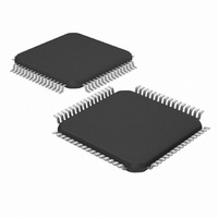
DSPIC33FJ32GS406-I/PT Microchip Technology, DSPIC33FJ32GS406-I/PT Datasheet - Page 119

DSPIC33FJ32GS406-I/PT
Manufacturer Part Number
DSPIC33FJ32GS406-I/PT
Description
IC MCU/DSP 32KB FLASH 64TQFP
Manufacturer
Microchip Technology
Series
dsPIC™ 33Fr
Specifications of DSPIC33FJ32GS406-I/PT
Core Processor
dsPIC
Core Size
16-Bit
Speed
40 MIPs
Connectivity
I²C, IrDA, LIN, SCI, SPI, UART/USART, USB
Peripherals
Brown-out Detect/Reset, QEI, POR, PWM, WDT
Number Of I /o
58
Program Memory Size
32KB (32K x 8)
Program Memory Type
FLASH
Ram Size
4K x 8
Voltage - Supply (vcc/vdd)
3 V ~ 3.6 V
Data Converters
A/D 16x10b
Oscillator Type
Internal
Operating Temperature
-40°C ~ 85°C
Package / Case
64-TFQFP
Core Frequency
40MHz
Embedded Interface Type
I2C, SPI, UART
No. Of I/o's
53
Flash Memory Size
32KB
Supply Voltage Range
3V To 3.6V
Rohs Compliant
Yes
Lead Free Status / RoHS Status
Lead free / RoHS Compliant
Eeprom Size
-
Lead Free Status / RoHS Status
Lead free / RoHS Compliant, Lead free / RoHS Compliant
Available stocks
Company
Part Number
Manufacturer
Quantity
Price
Company:
Part Number:
DSPIC33FJ32GS406-I/PT
Manufacturer:
Microchip Technology
Quantity:
10 000
- Current page: 119 of 418
- Download datasheet (3Mb)
6.2
A Power-on Reset (POR) circuit ensures the device is
reset from power-on. The POR circuit is active until
V
has elapsed. The delay, T
device bias circuits become stable.
The device supply voltage characteristics must meet
the
requirements
Section 27.0 “Electrical Characteristics” for details.
The POR Status (POR) bit in the Reset Control
(RCON<0>) register is set to indicate the Power-on
Reset.
6.3
The on-chip regulator has a Brown-out Reset (BOR)
circuit that resets the device when the V
(V
circuit keeps the device in Reset until V
FIGURE 6-3:
2010 Microchip Technology Inc.
DD
DD
dsPIC33FJ32GS406/606/608/610 and dsPIC33FJ64GS406/606/608/610
crosses the V
specified
< V
Power-on Reset (POR)
Brown-out Reset (BOR) and
Power-up Timer (PWRT)
BOR
SYSRST
) for proper device operation. The BOR
SYSRST
SYSRST
to
starting
V
V
V
POR
DD
generate the POR. Refer to
DD
DD
BROWN-OUT SITUATIONS
threshold and the delay, T
voltage
POR
V
DD
, ensures the internal
dips before PWRT expires
and
DD
DD
crosses the
rise
is too low
POR
rate
Preliminary
,
T
BOR
V
delay, T
becomes stable.
The BOR Status (BOR) bit in the Reset Control
(RCON<1>) register is set to indicate the Brown-out
Reset.
The device will not run at full speed after a BOR as the
V
operation. The PWRT provides power-up time delay
(T
stabilized at the appropriate levels for full-speed
operation before the SYSRST is released.
The power-up timer delay (T
the
(FPWRT<2:0>)
(FPOR<2:0>) register, which provides eight settings
(from 0 ms to 128 ms). Refer to Section 24.0 “Special
Features” for further details.
Figure 6-3 shows the typical brown-out scenarios. The
reset delay (T
rises above the V
BOR
DD
PWRT
+ T
T
T
PWRT
should rise to acceptable levels for full-speed
BOR
threshold and the delay, T
BOR
Power-on
) to ensure that the system power supplies have
BOR
+ T
+ T
, ensures the voltage regulator output
PWRT
PWRT
BOR
BOR
bits
+ T
Reset
PWRT
trip point
in
) is initiated each time V
the
PWRT
Timer
BOR
POR
) is programmed by
DS70591C-page 119
, has elapsed. The
V
V
V
BOR
BOR
BOR
Value
Configuration
Select
DD
Related parts for DSPIC33FJ32GS406-I/PT
Image
Part Number
Description
Manufacturer
Datasheet
Request
R

Part Number:
Description:
IC, DSC, 16BIT, 12KB, 40MHZ, 3.6V, DIP28
Manufacturer:
Microchip Technology
Datasheet:

Part Number:
Description:
Manufacturer:
Microchip Technology Inc.
Datasheet:

Part Number:
Description:
Manufacturer:
Microchip Technology Inc.
Datasheet:

Part Number:
Description:
Manufacturer:
Microchip Technology Inc.
Datasheet:

Part Number:
Description:
Manufacturer:
Microchip Technology Inc.
Datasheet:

Part Number:
Description:
Manufacturer:
Microchip Technology Inc.
Datasheet:

Part Number:
Description:
Manufacturer:
Microchip Technology Inc.
Datasheet:

Part Number:
Description:
Manufacturer:
Microchip Technology Inc.
Datasheet:

Part Number:
Description:
Manufacturer:
Microchip Technology Inc.
Datasheet:


