DSPIC33FJ32GS406-I/PT Microchip Technology, DSPIC33FJ32GS406-I/PT Datasheet - Page 253
DSPIC33FJ32GS406-I/PT
Manufacturer Part Number
DSPIC33FJ32GS406-I/PT
Description
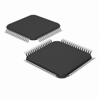
IC MCU/DSP 32KB FLASH 64TQFP
Manufacturer
Microchip Technology
Series
dsPIC™ 33Fr
Specifications of DSPIC33FJ32GS406-I/PT
Core Processor
dsPIC
Core Size
16-Bit
Speed
40 MIPs
Connectivity
I²C, IrDA, LIN, SCI, SPI, UART/USART, USB
Peripherals
Brown-out Detect/Reset, QEI, POR, PWM, WDT
Number Of I /o
58
Program Memory Size
32KB (32K x 8)
Program Memory Type
FLASH
Ram Size
4K x 8
Voltage - Supply (vcc/vdd)
3 V ~ 3.6 V
Data Converters
A/D 16x10b
Oscillator Type
Internal
Operating Temperature
-40°C ~ 85°C
Package / Case
64-TFQFP
Core Frequency
40MHz
Embedded Interface Type
I2C, SPI, UART
No. Of I/o's
53
Flash Memory Size
32KB
Supply Voltage Range
3V To 3.6V
Rohs Compliant
Yes
Lead Free Status / RoHS Status
Lead free / RoHS Compliant
Eeprom Size
-
Lead Free Status / RoHS Status
Lead free / RoHS Compliant, Lead free / RoHS Compliant
Available stocks
Company
Part Number
Manufacturer
Quantity
Price
Company:

Part Number:
DSPIC33FJ32GS406-I/PT
Manufacturer:
Microchip Technology
Quantity:
10 000


REGISTER 16-25: AUXCONx: PWM AUXILIARY CONTROL REGISTER
2010 Microchip Technology Inc.
bit 15
bit 7
Legend:
R = Readable bit
-n = Value at POR
bit 15
bit 14
bit 13-12
bit 11-8
bit 7-6
bit 5-2
bit 1
bit 0
dsPIC33FJ32GS406/606/608/610 and dsPIC33FJ64GS406/606/608/610
HRPDIS
R/W-0
U-0
—
HRPDIS: High Resolution PWM Period Disable bit
1 = High resolution PWM period is disabled to reduce power consumption
0 = High resolution PWM period is enabled
HRDDIS: High Resolution PWM Duty Cycle Disable bit
1 = High resolution PWM duty cycle is disabled to reduce power consumption
0 = High resolution PWM duty cycle is enabled
Unimplemented: Read as ‘0’
BLANKSEL<3:0>: PWM State Blank Source Select bits
The selected state blank signal will block the current limit and/or fault input signals
(if enabled via the BCH and BCL bits in the LEBCONx register)
1001 = PWM9H selected as state blank source
1000 = PWM8H selected as state blank source
0111 = PWM7H selected as state blank source
0110 = PWM6H selected as state blank source
0101 = PWM5H selected as state blank source
0100 = PWM4H selected as state blank source
0011 = PWM3H selected as state blank source
0010 = PWM2H selected as state blank source
0001 = PWM1H selected as state blank source
0000 = 1’b0 (no state blanking)
Unimplemented: Read as ‘0’
CHOPSEL<3:0>: PWM Chop Clock Source Select bits
The selected signal will enable and disable (CHOP) the selected PWM outputs
1001 = PWM9H selected as CHOP clock source
1000 = PWM8H selected as CHOP clock source
0111 = PWM7H selected as CHOP clock source
0110 = PWM6H selected as CHOP clock source
0101 = PWM5H selected as CHOP clock source
0100 = PWM4H selected as CHOP clock source
0011 = PWM3H selected as CHOP clock source
0010 = PWM2H selected as CHOP clock source
0001 = PWM1H selected as CHOP clock source
0000 = Chop Clock generator selected as CHOP clock source
CHOPHEN: PWMxH Output Chopping Enable bit
1 = PWMxH chopping function is enabled
0 = PWMxH chopping function is disabled
CHOPLEN: PWMxL Output Chopping Enable bit
1 = PWMxL chopping function is enabled
0 = PWMxL chopping function is disabled
HRDDIS
R/W-0
U-0
—
W = Writable bit
‘1’ = Bit is set
R/W-0
U-0
—
R/W-0
U-0
Preliminary
—
CHOPSEL<3:0>
U = Unimplemented bit, read as ‘0’
‘0’ = Bit is cleared
R/W-0
R/W-0
(1)
(1)
R/W-0
R/W-0
BLANKSEL<3:0>
x = Bit is unknown
CHOPHEN
R/W-0
R/W-0
DS70591C-page 253
CHOPLEN
R/W-0
R/W-0
bit 8
bit 0
Related parts for DSPIC33FJ32GS406-I/PT
Image
Part Number
Description
Manufacturer
Datasheet
Request
R

Part Number:
Description:
IC, DSC, 16BIT, 12KB, 40MHZ, 3.6V, DIP28
Manufacturer:
Microchip Technology
Datasheet:

Part Number:
Description:
Manufacturer:
Microchip Technology Inc.
Datasheet:
Part Number:
Description:
Manufacturer:
Microchip Technology Inc.
Datasheet:
Part Number:
Description:
Manufacturer:
Microchip Technology Inc.
Datasheet:
Part Number:
Description:
Manufacturer:
Microchip Technology Inc.
Datasheet:
Part Number:
Description:
Manufacturer:
Microchip Technology Inc.
Datasheet:
Part Number:
Description:
Manufacturer:
Microchip Technology Inc.
Datasheet:
Part Number:
Description:
Manufacturer:
Microchip Technology Inc.
Datasheet:
Part Number:
Description:
Manufacturer:
Microchip Technology Inc.
Datasheet: