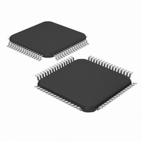
DSPIC33FJ32GS406-I/PT Microchip Technology, DSPIC33FJ32GS406-I/PT Datasheet - Page 311

DSPIC33FJ32GS406-I/PT
Manufacturer Part Number
DSPIC33FJ32GS406-I/PT
Description
IC MCU/DSP 32KB FLASH 64TQFP
Manufacturer
Microchip Technology
Series
dsPIC™ 33Fr
Specifications of DSPIC33FJ32GS406-I/PT
Core Processor
dsPIC
Core Size
16-Bit
Speed
40 MIPs
Connectivity
I²C, IrDA, LIN, SCI, SPI, UART/USART, USB
Peripherals
Brown-out Detect/Reset, QEI, POR, PWM, WDT
Number Of I /o
58
Program Memory Size
32KB (32K x 8)
Program Memory Type
FLASH
Ram Size
4K x 8
Voltage - Supply (vcc/vdd)
3 V ~ 3.6 V
Data Converters
A/D 16x10b
Oscillator Type
Internal
Operating Temperature
-40°C ~ 85°C
Package / Case
64-TFQFP
Core Frequency
40MHz
Embedded Interface Type
I2C, SPI, UART
No. Of I/o's
53
Flash Memory Size
32KB
Supply Voltage Range
3V To 3.6V
Rohs Compliant
Yes
Lead Free Status / RoHS Status
Lead free / RoHS Compliant
Eeprom Size
-
Lead Free Status / RoHS Status
Lead free / RoHS Compliant, Lead free / RoHS Compliant
Available stocks
Company
Part Number
Manufacturer
Quantity
Price
Company:
Part Number:
DSPIC33FJ32GS406-I/PT
Manufacturer:
Microchip Technology
Quantity:
10 000
- Current page: 311 of 418
- Download datasheet (3Mb)
REGISTER 22-1:
2010 Microchip Technology Inc.
bit 15
bit 7
Legend:
R = Readable bit
-n = Value at POR
bit 15
bit 14
bit 13
bit 12
bit 11
bit 10
bit 9
bit 8
bit 7
bit 6
bit 5
bit 4
dsPIC33FJ32GS406/606/608/610 and dsPIC33FJ64GS406/606/608/610
Note 1: This control bit can only be changed while the ADC is disabled (ADON = 0).
ADON
R/W-0
R/W-0
EIE
(1)
ADON: A/D Operating Mode bit
1 = A/D converter module is operating
0 = A/D converter is off
Unimplemented: Read as ‘0’
ADSIDL: Stop in Idle Mode bit
1 = Discontinue module operation when device enters Idle mode
0 = Continue module operation in Idle mode
SLOWCLK: Enable The Slow Clock Divider bit
1 = ADC is clocked by the auxiliary PLL (ACLK)
0 = ADC is clock by the primary PLL (F
Unimplemented: Read as ‘0’
GSWTRG: Global Software Trigger bit
When this bit is set by the user, it will trigger conversions if selected by the TRGSRC<4:0> bits in the
ADCPCx registers. This bit must be cleared by the user prior to initiating another global trigger (i.e., this
bit is not auto-clearing).
Unimplemented: Read as ‘0’
FORM: Data Output Format bit
1 = Fractional (D
0 = Integer (D
EIE: Early Interrupt Enable bit
1 = Interrupt is generated after first conversion is completed
0 = Interrupt is generated after second conversion is completed
ORDER: Conversion Order bit
1 = Odd numbered analog input is converted first, followed by conversion of even numbered input
0 = Even numbered analog input is converted first, followed by conversion of odd numbered input
SEQSAMP: Sequential Sample Enable bit
1 = Shared Sample and Hold (S&H) circuit is sampled at the start of the second conversion if
0 = Shared S&H is sampled at the same time the dedicated S&H is sampled if the shared S&H is not
ASYNCSAMP: Asynchronous Dedicated S&H Sampling Enable bit
1 = The dedicated S&H is constantly sampling and then terminates sampling as soon as the trigger
0 = The dedicated S&H starts sampling when the trigger event is detected and completes the sampling
ORDER
R/W-0
U-0
ORDER = 0. If ORDER = 1, then the shared S&H is sampled at the start of the first conversion.
currently busy with an existing conversion process. If the shared S&H is busy at the time the
dedicated S&H is sampled, then the shared S&H will sample at the start of the new conversion
cycle.
pulse is detected.
process in two ADC clock cycles.
—
ADCON: A/D CONTROL REGISTER
(1)
W = Writable bit
‘1’ = Bit is set
SEQSAMP
OUT
ADSIDL
OUT
R/W-0
R/W-0
= 0000 00dd dddd dddd)
= dddd dddd dd00 0000)
(1)
ASYNCSAMP
(1)
(1)
SLOWCLK
(1)
R/W-0
R/W-0
Preliminary
VCO
(1)
(1)
(1)
)
(1)
U = Unimplemented bit, read as ‘0’
‘0’ = Bit is cleared
U-0
U-0
—
—
GSWTRG
R/W-0
R/W-0
(1)
ADCS<2:0>
x = Bit is unknown
R/W-1
U-0
—
DS70591C-page 311
(1)
FORM
R/W-0
R/W-1
bit 8
bit 0
(1)
Related parts for DSPIC33FJ32GS406-I/PT
Image
Part Number
Description
Manufacturer
Datasheet
Request
R

Part Number:
Description:
IC, DSC, 16BIT, 12KB, 40MHZ, 3.6V, DIP28
Manufacturer:
Microchip Technology
Datasheet:

Part Number:
Description:
Manufacturer:
Microchip Technology Inc.
Datasheet:

Part Number:
Description:
Manufacturer:
Microchip Technology Inc.
Datasheet:

Part Number:
Description:
Manufacturer:
Microchip Technology Inc.
Datasheet:

Part Number:
Description:
Manufacturer:
Microchip Technology Inc.
Datasheet:

Part Number:
Description:
Manufacturer:
Microchip Technology Inc.
Datasheet:

Part Number:
Description:
Manufacturer:
Microchip Technology Inc.
Datasheet:

Part Number:
Description:
Manufacturer:
Microchip Technology Inc.
Datasheet:

Part Number:
Description:
Manufacturer:
Microchip Technology Inc.
Datasheet:


