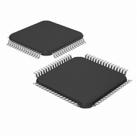
DSPIC33FJ32GS406-I/PT Microchip Technology, DSPIC33FJ32GS406-I/PT Datasheet - Page 213

DSPIC33FJ32GS406-I/PT
Manufacturer Part Number
DSPIC33FJ32GS406-I/PT
Description
IC MCU/DSP 32KB FLASH 64TQFP
Manufacturer
Microchip Technology
Series
dsPIC™ 33Fr
Specifications of DSPIC33FJ32GS406-I/PT
Core Processor
dsPIC
Core Size
16-Bit
Speed
40 MIPs
Connectivity
I²C, IrDA, LIN, SCI, SPI, UART/USART, USB
Peripherals
Brown-out Detect/Reset, QEI, POR, PWM, WDT
Number Of I /o
58
Program Memory Size
32KB (32K x 8)
Program Memory Type
FLASH
Ram Size
4K x 8
Voltage - Supply (vcc/vdd)
3 V ~ 3.6 V
Data Converters
A/D 16x10b
Oscillator Type
Internal
Operating Temperature
-40°C ~ 85°C
Package / Case
64-TFQFP
Core Frequency
40MHz
Embedded Interface Type
I2C, SPI, UART
No. Of I/o's
53
Flash Memory Size
32KB
Supply Voltage Range
3V To 3.6V
Rohs Compliant
Yes
Lead Free Status / RoHS Status
Lead free / RoHS Compliant
Eeprom Size
-
Lead Free Status / RoHS Status
Lead free / RoHS Compliant, Lead free / RoHS Compliant
Available stocks
Company
Part Number
Manufacturer
Quantity
Price
Company:
Part Number:
DSPIC33FJ32GS406-I/PT
Manufacturer:
Microchip Technology
Quantity:
10 000
- Current page: 213 of 418
- Download datasheet (3Mb)
13.0
Timer2 and Timer4 are Type B timers that offer the
following major features:
FIGURE 13-1:
FIGURE 13-2:
2010 Microchip Technology Inc.
dsPIC33FJ32GS406/606/608/610 and dsPIC33FJ64GS406/606/608/610
Note 1: This data sheet summarizes the features
2: Some registers and associated bits
TIMER2/3/4/5 FEATURES
TxCK
TxCK
of the dsPIC33FJ32GS406/606/608/610
and
families of devices. It is not intended to be
a comprehensive reference source. To
complement the information in this data
sheet, refer to Section 11. “Timers”
(DS70205) in the “dsPIC33F/PIC24H
Family Reference Manual”, which is avail-
able from the Microchip web site
(www.microchip.com).
described in this section may not be avail-
able on all devices. Refer to Section 4.0
“Memory Organization” in this data
sheet for device-specific register and bit
information.
dsPIC33FJ64GS406/606/608/610
TYPE B TIMER BLOCK DIAGRAM (x = 2, 4)
TYPE C TIMER BLOCK DIAGRAM (x = 3, 5)
F
CY
Sync
TCKPS<1:0>
Prescaler
(/n)
F
CY
TCKPS<1:0>
TCKPS<1:0>
TCKPS<1:0>
Prescaler
Prescaler
Prescaler
Sync
Gate
(/n)
Sync
(/n)
Gate
Sync
(/n)
Preliminary
Falling Edge
Falling Edge
Detect
TGATE
Detect
TCS
TGATE
TCS
• A Type B timer can be concatenated with a
• External clock input (TxCK) is always synchronized
Figure 13-1 shows a block diagram of the Type B timer.
Timer3 and Timer5 are Type C timers that offer the
following major features:
• A Type C timer can be concatenated with a
• At least one Type C timer has the ability to trigger
• The external clock input (TxCK) is always
A block diagram of the Type C timer is shown in
Figure 13-2.
10
00
x1
Type C timer to form a 32-bit timer
to the internal device clock and the clock
synchronization is performed after the prescaler.
Type B timer to form a 32-bit timer
an A/D conversion.
synchronized to the internal device clock and the
clock synchronization is performed before the
prescaler
Note:
10
00
x1
Comparator
Comparator
Timer3 is not available on all devices.
TMRx
TMRx
PRx
PRx
Reset
Equal
Equal
Reset
TGATE
ADC SOC Trigger
TGATE
1
0
1
0
Set TxIF Flag
Set TxIF Flag
DS70591C-page 213
Related parts for DSPIC33FJ32GS406-I/PT
Image
Part Number
Description
Manufacturer
Datasheet
Request
R

Part Number:
Description:
IC, DSC, 16BIT, 12KB, 40MHZ, 3.6V, DIP28
Manufacturer:
Microchip Technology
Datasheet:

Part Number:
Description:
Manufacturer:
Microchip Technology Inc.
Datasheet:

Part Number:
Description:
Manufacturer:
Microchip Technology Inc.
Datasheet:

Part Number:
Description:
Manufacturer:
Microchip Technology Inc.
Datasheet:

Part Number:
Description:
Manufacturer:
Microchip Technology Inc.
Datasheet:

Part Number:
Description:
Manufacturer:
Microchip Technology Inc.
Datasheet:

Part Number:
Description:
Manufacturer:
Microchip Technology Inc.
Datasheet:

Part Number:
Description:
Manufacturer:
Microchip Technology Inc.
Datasheet:

Part Number:
Description:
Manufacturer:
Microchip Technology Inc.
Datasheet:


