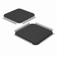
DSPIC33FJ32GS406-I/PT Microchip Technology, DSPIC33FJ32GS406-I/PT Datasheet - Page 221

DSPIC33FJ32GS406-I/PT
Manufacturer Part Number
DSPIC33FJ32GS406-I/PT
Description
IC MCU/DSP 32KB FLASH 64TQFP
Manufacturer
Microchip Technology
Series
dsPIC™ 33Fr
Specifications of DSPIC33FJ32GS406-I/PT
Core Processor
dsPIC
Core Size
16-Bit
Speed
40 MIPs
Connectivity
I²C, IrDA, LIN, SCI, SPI, UART/USART, USB
Peripherals
Brown-out Detect/Reset, QEI, POR, PWM, WDT
Number Of I /o
58
Program Memory Size
32KB (32K x 8)
Program Memory Type
FLASH
Ram Size
4K x 8
Voltage - Supply (vcc/vdd)
3 V ~ 3.6 V
Data Converters
A/D 16x10b
Oscillator Type
Internal
Operating Temperature
-40°C ~ 85°C
Package / Case
64-TFQFP
Core Frequency
40MHz
Embedded Interface Type
I2C, SPI, UART
No. Of I/o's
53
Flash Memory Size
32KB
Supply Voltage Range
3V To 3.6V
Rohs Compliant
Yes
Lead Free Status / RoHS Status
Lead free / RoHS Compliant
Eeprom Size
-
Lead Free Status / RoHS Status
Lead free / RoHS Compliant, Lead free / RoHS Compliant
Available stocks
Company
Part Number
Manufacturer
Quantity
Price
Company:
Part Number:
DSPIC33FJ32GS406-I/PT
Manufacturer:
Microchip Technology
Quantity:
10 000
- Current page: 221 of 418
- Download datasheet (3Mb)
15.0
FIGURE 15-1:
2010 Microchip Technology Inc.
dsPIC33FJ32GS406/606/608/610 and dsPIC33FJ64GS406/606/608/610
Note 1: This data sheet summarizes the features
2: Some registers and associated bits
OUTPUT COMPARE
Note: An ‘x’ in a signal, register or bit name denotes the number of the output compare channels.
of the dsPIC33FJ32GS406/606/608/610
and
families of devices. It is not intended to be
a comprehensive reference source. To
complement the information in this data
sheet, refer to Section 13. “Output
Compare” (DS70209) in the “dsPIC33F/
PIC24H
which is available from the Microchip web
site (www.microchip.com).
described in this section may not be avail-
able on all devices. Refer to Section 4.0
“Memory Organization” in this data
sheet for device-specific register and bit
information.
dsPIC33FJ64GS406/606/608/610
OUTPUT COMPARE MODULE BLOCK DIAGRAM
Family
16
TMR2
Comparator
0
OCxRS
OCxR
Reference
TMR3
1
16
OCTSEL
Manual”,
Rollover Rollover
Preliminary
TMR2
0
TMR3
1
The output compare module can select either Timer2 or
Timer3 for its time base. The module compares the
value of the timer with the value of one or two Compare
registers depending on the operating mode selected.
The state of the output pin changes when the timer
value matches the Compare register value. The output
compare module generates either a single output
pulse, or a sequence of output pulses, by changing the
state of the output pin on the compare match events.
The output compare module can also generate
interrupts on compare match events.
The output compare module has multiple operating
modes:
• Active-Low One-Shot mode
• Active-High One-Shot mode
• Toggle mode
• Delayed One-Shot mode
• Continuous Pulse mode
• PWM mode without Fault Protection
• PWM mode with Fault Protection
Mode Select
OCM<2:0>
Output
Logic
3
Set Flag bit
OCxIF
R
S
Q
Output Enable
DS70591C-page 221
OCx
OCFA
Related parts for DSPIC33FJ32GS406-I/PT
Image
Part Number
Description
Manufacturer
Datasheet
Request
R

Part Number:
Description:
IC, DSC, 16BIT, 12KB, 40MHZ, 3.6V, DIP28
Manufacturer:
Microchip Technology
Datasheet:

Part Number:
Description:
Manufacturer:
Microchip Technology Inc.
Datasheet:

Part Number:
Description:
Manufacturer:
Microchip Technology Inc.
Datasheet:

Part Number:
Description:
Manufacturer:
Microchip Technology Inc.
Datasheet:

Part Number:
Description:
Manufacturer:
Microchip Technology Inc.
Datasheet:

Part Number:
Description:
Manufacturer:
Microchip Technology Inc.
Datasheet:

Part Number:
Description:
Manufacturer:
Microchip Technology Inc.
Datasheet:

Part Number:
Description:
Manufacturer:
Microchip Technology Inc.
Datasheet:

Part Number:
Description:
Manufacturer:
Microchip Technology Inc.
Datasheet:


