MC9S12E256MFUE Freescale Semiconductor, MC9S12E256MFUE Datasheet - Page 104
MC9S12E256MFUE
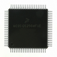
Manufacturer Part Number
MC9S12E256MFUE
Description
IC MCU 256K FLASH 25MHZ 80-QFP
Manufacturer
Freescale Semiconductor
Series
HCS12r
Specifications of MC9S12E256MFUE
Core Processor
HCS12
Core Size
16-Bit
Speed
25MHz
Connectivity
EBI/EMI, I²C, SCI, SPI
Peripherals
POR, PWM, WDT
Number Of I /o
60
Program Memory Size
256KB (256K x 8)
Program Memory Type
FLASH
Ram Size
16K x 8
Voltage - Supply (vcc/vdd)
2.35 V ~ 2.75 V
Data Converters
A/D 16x10b; D/A 2x8b
Oscillator Type
Internal
Operating Temperature
-40°C ~ 125°C
Package / Case
80-QFP
Processor Series
S12E
Core
HCS12
Data Bus Width
16 bit
Data Ram Size
16 KB
Interface Type
I2C/SCI/SPI
Maximum Clock Frequency
50 MHz
Number Of Programmable I/os
60
Number Of Timers
12
Operating Supply Voltage
0 V to 5 V
Maximum Operating Temperature
+ 125 C
Mounting Style
SMD/SMT
3rd Party Development Tools
EWHCS12
Minimum Operating Temperature
- 40 C
On-chip Adc
16-ch x 10-bit
On-chip Dac
2-ch x 8-bit
Controller Family/series
HCS12/S12X
No. Of I/o's
60
Ram Memory Size
16KB
Cpu Speed
25MHz
No. Of Timers
3
Embedded Interface Type
I2C, SCI, SPI
Rohs Compliant
Yes
For Use With
M68EVB912E128 - BOARD EVAL FOR MC9S12E128/64
Lead Free Status / RoHS Status
Lead free / RoHS Compliant
Eeprom Size
-
Lead Free Status / Rohs Status
Lead free / RoHS Compliant
Available stocks
Company
Part Number
Manufacturer
Quantity
Price
Company:

Part Number:
MC9S12E256MFUE
Manufacturer:
FREESCAL
Quantity:
329
Company:
Part Number:
MC9S12E256MFUE
Manufacturer:
Freescale Semiconductor
Quantity:
10 000


Chapter 2 256 Kbyte Flash Module (FTS256K2V1)
2.4.1.2
The Flash command controller is used to supervise the command write sequence to execute program,
erase, erase verify, and data compress algorithms.
Before starting a command write sequence, the ACCERR and PVIOL flags in the FSTAT register must be
clear (see
determine the state of the address, data, and command buffers. If the CBEIF flag is set, indicating the
buffers are empty, a new command write sequence can be started. If the CBEIF flag is clear, indicating the
buffers are not available, a new command write sequence will overwrite the contents of the address, data,
and command buffers.
A command write sequence consists of three steps which must be strictly adhered to with writes to the
Flash module not permitted between the steps. However, Flash register and array reads are allowed during
a command write sequence. A command write sequence consists of the following steps:
A command write sequence can be aborted prior to clearing the CBEIF flag by writing a 0 to the CBEIF
flag and will result in the ACCERR flag being set.
104
1. Write an aligned data word to a valid Flash array address. The address and data will be stored in
2. Write a valid command to the FCMD register.
3. Clear the CBEIF flag by writing a 1 to CBEIF to launch the command. When the CBEIF flag is
the address and data buffers, respectively. If the CBEIF flag is clear when the Flash array write
occurs, the contents of the address and data buffers will be overwritten and the CBEIF flag will be
set.
a) For the erase verify command (see
b) For the data compress command (see
c) For the program command (see
d) For the sector erase command (see
e) For the mass erase command (see
f) For the sector erase abort command (see
cleared, the CCIF flag is cleared on the same bus cycle by internal hardware indicating that the
command was successfully launched. For all command write sequences except data compress and
sector erase abort, the CBEIF flag will set four bus cycles after the CCIF flag is cleared indicating
that the address, data, and command buffers are ready for a new command write sequence to begin.
For data compress and sector erase abort operations, the CBEIF flag will remain clear until the
operation completes.
Section 2.3.2.7, “Flash Status Register
of the data buffer are ignored and all address bits in the address buffer are ignored.
contents of the data buffer represents the number of consecutive words to read for data
compression and the contents of the address buffer represents the starting address.
data buffer will be programmed to the address specified in the address buffer with all address
bits valid.
of the data buffer are ignored and address bits [9:0] contained in the address buffer are ignored.
the data buffer and address buffer are ignored.
the contents of the data buffer and address buffer are ignored.
Command Write Sequence
MC9S12E256 Data Sheet, Rev. 1.08
Section 2.4.1.3.3, “Program
Section 2.4.1.3.5, “Mass Erase
Section 2.4.1.3.1, “Erase Verify
Section 2.4.1.3.4, “Sector Erase
Section 2.4.1.3.2, “Data Compress
(FSTAT)”) and the CBEIF flag must be tested to
Section 2.4.1.3.6, “Sector Erase Abort
Command”), the contents of the
Command”), the contents of
Command”), the contents
Command”), the contents
Freescale Semiconductor
Command”), the
Command”),
Related parts for MC9S12E256MFUE
Image
Part Number
Description
Manufacturer
Datasheet
Request
R

Part Number:
Description:
Manufacturer:
Freescale Semiconductor, Inc
Datasheet:
Part Number:
Description:
Manufacturer:
Freescale Semiconductor, Inc
Datasheet:
Part Number:
Description:
Manufacturer:
Freescale Semiconductor, Inc
Datasheet:
Part Number:
Description:
Manufacturer:
Freescale Semiconductor, Inc
Datasheet:
Part Number:
Description:
Manufacturer:
Freescale Semiconductor, Inc
Datasheet:
Part Number:
Description:
Manufacturer:
Freescale Semiconductor, Inc
Datasheet:
Part Number:
Description:
Manufacturer:
Freescale Semiconductor, Inc
Datasheet:
Part Number:
Description:
Manufacturer:
Freescale Semiconductor, Inc
Datasheet:
Part Number:
Description:
Manufacturer:
Freescale Semiconductor, Inc
Datasheet:
Part Number:
Description:
Manufacturer:
Freescale Semiconductor, Inc
Datasheet:
Part Number:
Description:
Manufacturer:
Freescale Semiconductor, Inc
Datasheet:
Part Number:
Description:
Manufacturer:
Freescale Semiconductor, Inc
Datasheet:
Part Number:
Description:
Manufacturer:
Freescale Semiconductor, Inc
Datasheet:
Part Number:
Description:
Manufacturer:
Freescale Semiconductor, Inc
Datasheet:
Part Number:
Description:
Manufacturer:
Freescale Semiconductor, Inc
Datasheet: