MC9S12E256MFUE Freescale Semiconductor, MC9S12E256MFUE Datasheet - Page 516
MC9S12E256MFUE
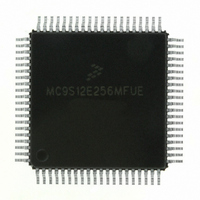
Manufacturer Part Number
MC9S12E256MFUE
Description
IC MCU 256K FLASH 25MHZ 80-QFP
Manufacturer
Freescale Semiconductor
Series
HCS12r
Specifications of MC9S12E256MFUE
Core Processor
HCS12
Core Size
16-Bit
Speed
25MHz
Connectivity
EBI/EMI, I²C, SCI, SPI
Peripherals
POR, PWM, WDT
Number Of I /o
60
Program Memory Size
256KB (256K x 8)
Program Memory Type
FLASH
Ram Size
16K x 8
Voltage - Supply (vcc/vdd)
2.35 V ~ 2.75 V
Data Converters
A/D 16x10b; D/A 2x8b
Oscillator Type
Internal
Operating Temperature
-40°C ~ 125°C
Package / Case
80-QFP
Processor Series
S12E
Core
HCS12
Data Bus Width
16 bit
Data Ram Size
16 KB
Interface Type
I2C/SCI/SPI
Maximum Clock Frequency
50 MHz
Number Of Programmable I/os
60
Number Of Timers
12
Operating Supply Voltage
0 V to 5 V
Maximum Operating Temperature
+ 125 C
Mounting Style
SMD/SMT
3rd Party Development Tools
EWHCS12
Minimum Operating Temperature
- 40 C
On-chip Adc
16-ch x 10-bit
On-chip Dac
2-ch x 8-bit
Controller Family/series
HCS12/S12X
No. Of I/o's
60
Ram Memory Size
16KB
Cpu Speed
25MHz
No. Of Timers
3
Embedded Interface Type
I2C, SCI, SPI
Rohs Compliant
Yes
For Use With
M68EVB912E128 - BOARD EVAL FOR MC9S12E128/64
Lead Free Status / RoHS Status
Lead free / RoHS Compliant
Eeprom Size
-
Lead Free Status / Rohs Status
Lead free / RoHS Compliant
Available stocks
Company
Part Number
Manufacturer
Quantity
Price
Company:

Part Number:
MC9S12E256MFUE
Manufacturer:
FREESCAL
Quantity:
329
Company:
Part Number:
MC9S12E256MFUE
Manufacturer:
Freescale Semiconductor
Quantity:
10 000


Chapter 18 Multiplexed External Bus Interface (MEBIV3)
18.3.2.1
Read: Anytime when register is in the map
Write: Anytime when register is in the map
Port A bits 7 through 0 are associated with address lines A15 through A8 respectively and data lines
D15/D7 through D8/D0 respectively. When this port is not used for external addresses such as in
single-chip mode, these pins can be used as general-purpose I/O. Data direction register A (DDRA)
determines the primary direction of each pin. DDRA also determines the source of data for a read of
PORTA.
This register is not in the on-chip memory map in expanded and special peripheral modes. Therefore, these
accesses will be echoed externally.
516
Emulation Narrow with
IVIS, and Peripheral
Expanded Narrow AB15 and
Expanded Wide,
Single Chip
Port A Data Register (PORTA)
To ensure that you read the value present on the PORTA pins, always wait
at least one cycle after writing to the DDRA register before reading from the
PORTA register.
Reset
W
R
DB15/DB7
AB/DB15
Bit 7
PA7
0
7
Figure 18-3. Port A Data Register (PORTA)
DB14/DB6
AB14 and
AB/DB14
PA6
6
0
6
MC9S12E256 Data Sheet, Rev. 1.08
DB13/DB5
AB13 and
AB/DB13
PA5
5
0
5
NOTE
DB12/DB4
AB12 and
AB/DB12
PA4
4
4
0
DB11/DB3
AB11 and
AB/DB11
PA3
3
0
3
DB10/DB2
AB10 and
AB/DB10
PA2
2
0
2
Freescale Semiconductor
DB9/DB1
AB9 and
AB/DB9
PA1
1
0
1
DB8/DB0
AB8 and
AB/DB8
Bit 0
PA0
0
0
Related parts for MC9S12E256MFUE
Image
Part Number
Description
Manufacturer
Datasheet
Request
R

Part Number:
Description:
Manufacturer:
Freescale Semiconductor, Inc
Datasheet:
Part Number:
Description:
Manufacturer:
Freescale Semiconductor, Inc
Datasheet:
Part Number:
Description:
Manufacturer:
Freescale Semiconductor, Inc
Datasheet:
Part Number:
Description:
Manufacturer:
Freescale Semiconductor, Inc
Datasheet:
Part Number:
Description:
Manufacturer:
Freescale Semiconductor, Inc
Datasheet:
Part Number:
Description:
Manufacturer:
Freescale Semiconductor, Inc
Datasheet:
Part Number:
Description:
Manufacturer:
Freescale Semiconductor, Inc
Datasheet:
Part Number:
Description:
Manufacturer:
Freescale Semiconductor, Inc
Datasheet:
Part Number:
Description:
Manufacturer:
Freescale Semiconductor, Inc
Datasheet:
Part Number:
Description:
Manufacturer:
Freescale Semiconductor, Inc
Datasheet:
Part Number:
Description:
Manufacturer:
Freescale Semiconductor, Inc
Datasheet:
Part Number:
Description:
Manufacturer:
Freescale Semiconductor, Inc
Datasheet:
Part Number:
Description:
Manufacturer:
Freescale Semiconductor, Inc
Datasheet:
Part Number:
Description:
Manufacturer:
Freescale Semiconductor, Inc
Datasheet:
Part Number:
Description:
Manufacturer:
Freescale Semiconductor, Inc
Datasheet: