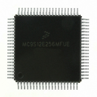
MC9S12E256MFUE Freescale Semiconductor, MC9S12E256MFUE Datasheet - Page 272

MC9S12E256MFUE
Manufacturer Part Number
MC9S12E256MFUE
Description
IC MCU 256K FLASH 25MHZ 80-QFP
Manufacturer
Freescale Semiconductor
Series
HCS12r
Specifications of MC9S12E256MFUE
Core Processor
HCS12
Core Size
16-Bit
Speed
25MHz
Connectivity
EBI/EMI, I²C, SCI, SPI
Peripherals
POR, PWM, WDT
Number Of I /o
60
Program Memory Size
256KB (256K x 8)
Program Memory Type
FLASH
Ram Size
16K x 8
Voltage - Supply (vcc/vdd)
2.35 V ~ 2.75 V
Data Converters
A/D 16x10b; D/A 2x8b
Oscillator Type
Internal
Operating Temperature
-40°C ~ 125°C
Package / Case
80-QFP
Processor Series
S12E
Core
HCS12
Data Bus Width
16 bit
Data Ram Size
16 KB
Interface Type
I2C/SCI/SPI
Maximum Clock Frequency
50 MHz
Number Of Programmable I/os
60
Number Of Timers
12
Operating Supply Voltage
0 V to 5 V
Maximum Operating Temperature
+ 125 C
Mounting Style
SMD/SMT
3rd Party Development Tools
EWHCS12
Minimum Operating Temperature
- 40 C
On-chip Adc
16-ch x 10-bit
On-chip Dac
2-ch x 8-bit
Controller Family/series
HCS12/S12X
No. Of I/o's
60
Ram Memory Size
16KB
Cpu Speed
25MHz
No. Of Timers
3
Embedded Interface Type
I2C, SCI, SPI
Rohs Compliant
Yes
For Use With
M68EVB912E128 - BOARD EVAL FOR MC9S12E128/64
Lead Free Status / RoHS Status
Lead free / RoHS Compliant
Eeprom Size
-
Lead Free Status / Rohs Status
Lead free / RoHS Compliant
Available stocks
Company
Part Number
Manufacturer
Quantity
Price
Company:
Part Number:
MC9S12E256MFUE
Manufacturer:
FREESCAL
Quantity:
329
Company:
Part Number:
MC9S12E256MFUE
Manufacturer:
Freescale Semiconductor
Quantity:
10 000
- Current page: 272 of 602
- Download datasheet (4Mb)
Chapter 8 Serial Communication Interface (SCIV4)
Enable single-wire operation by setting the LOOPS bit and the receiver source bit, RSRC, in SCI control
register 1 (SCICR1). Setting the LOOPS bit disables the path from the RXD pin to the receiver. Setting
the RSRC bit connects the TXD pin to the receiver. Both the transmitter and receiver must be enabled
(TE = 1 and RE = 1).The TXDIR bit (SCISR2[1]) determines whether the TXD pin is going to be used as
an input (TXDIR = 0) or an output (TXDIR = 1) in this mode of operation.
8.4.7
In loop operation the transmitter output goes to the receiver input. The RXD pin is disconnected from the
SCI
Enable loop operation by setting the LOOPS bit and clearing the RSRC bit in SCI control register 1
(SCICR1). Setting the LOOPS bit disables the path from the RXD pin to the receiver. Clearing the RSRC
bit connects the transmitter output to the receiver input. Both the transmitter and receiver must be enabled
(TE = 1 and RE = 1).
8.5
This section describes the interrupt originated by the SCI block.The MCU must service the interrupt
requests.
272
Interrupt
.
TDRE
RDRF
IDLE
OR
TC
Table 8-17
Interrupts
Loop Operation
SCISR1[7]
SCISR1[6]
SCISR1[5]
SCISR1[3]
SCISR1[4]
In single-wire operation data from the TXD pin is inverted if RXPOL is set.
In loop operation data from the transmitter is not recognized by the receiver
if RXPOL and TXPOL are not the same.
Source
lists the five interrupt sources of the SCI.
Figure 8-25. Loop Operation (LOOPS = 1, RSRC = 0)
Local Enable
TCIE
ILIE
RIE
TIE
TRANSMITTER
RECEIVER
Table 8-17. SCI Interrupt Sources
MC9S12E256 Data Sheet, Rev. 1.08
Active high level. Indicates that a byte was transferred from SCIDRH/L to
the transmit shift register.
Active high level. Indicates that a transmit is complete.
Active high level. The RDRF interrupt indicates that received data is
available in the SCI data register.
occurred.
Active high level. Indicates that receiver input has become idle.
Active high level. This interrupt indicates that an overrun condition has
NOTE
NOTE
RXD
TXD
Description
Freescale Semiconductor
Related parts for MC9S12E256MFUE
Image
Part Number
Description
Manufacturer
Datasheet
Request
R
Part Number:
Description:
Manufacturer:
Freescale Semiconductor, Inc
Datasheet:
Part Number:
Description:
Manufacturer:
Freescale Semiconductor, Inc
Datasheet:
Part Number:
Description:
Manufacturer:
Freescale Semiconductor, Inc
Datasheet:
Part Number:
Description:
Manufacturer:
Freescale Semiconductor, Inc
Datasheet:
Part Number:
Description:
Manufacturer:
Freescale Semiconductor, Inc
Datasheet:
Part Number:
Description:
Manufacturer:
Freescale Semiconductor, Inc
Datasheet:
Part Number:
Description:
Manufacturer:
Freescale Semiconductor, Inc
Datasheet:
Part Number:
Description:
Manufacturer:
Freescale Semiconductor, Inc
Datasheet:
Part Number:
Description:
Manufacturer:
Freescale Semiconductor, Inc
Datasheet:
Part Number:
Description:
Manufacturer:
Freescale Semiconductor, Inc
Datasheet:
Part Number:
Description:
Manufacturer:
Freescale Semiconductor, Inc
Datasheet:
Part Number:
Description:
Manufacturer:
Freescale Semiconductor, Inc
Datasheet:
Part Number:
Description:
Manufacturer:
Freescale Semiconductor, Inc
Datasheet:
Part Number:
Description:
Manufacturer:
Freescale Semiconductor, Inc
Datasheet:
Part Number:
Description:
Manufacturer:
Freescale Semiconductor, Inc
Datasheet:


