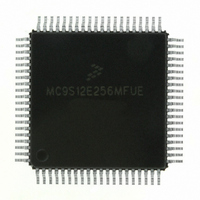
MC9S12E256MFUE Freescale Semiconductor, MC9S12E256MFUE Datasheet - Page 147

MC9S12E256MFUE
Manufacturer Part Number
MC9S12E256MFUE
Description
IC MCU 256K FLASH 25MHZ 80-QFP
Manufacturer
Freescale Semiconductor
Series
HCS12r
Specifications of MC9S12E256MFUE
Core Processor
HCS12
Core Size
16-Bit
Speed
25MHz
Connectivity
EBI/EMI, I²C, SCI, SPI
Peripherals
POR, PWM, WDT
Number Of I /o
60
Program Memory Size
256KB (256K x 8)
Program Memory Type
FLASH
Ram Size
16K x 8
Voltage - Supply (vcc/vdd)
2.35 V ~ 2.75 V
Data Converters
A/D 16x10b; D/A 2x8b
Oscillator Type
Internal
Operating Temperature
-40°C ~ 125°C
Package / Case
80-QFP
Processor Series
S12E
Core
HCS12
Data Bus Width
16 bit
Data Ram Size
16 KB
Interface Type
I2C/SCI/SPI
Maximum Clock Frequency
50 MHz
Number Of Programmable I/os
60
Number Of Timers
12
Operating Supply Voltage
0 V to 5 V
Maximum Operating Temperature
+ 125 C
Mounting Style
SMD/SMT
3rd Party Development Tools
EWHCS12
Minimum Operating Temperature
- 40 C
On-chip Adc
16-ch x 10-bit
On-chip Dac
2-ch x 8-bit
Controller Family/series
HCS12/S12X
No. Of I/o's
60
Ram Memory Size
16KB
Cpu Speed
25MHz
No. Of Timers
3
Embedded Interface Type
I2C, SCI, SPI
Rohs Compliant
Yes
For Use With
M68EVB912E128 - BOARD EVAL FOR MC9S12E128/64
Lead Free Status / RoHS Status
Lead free / RoHS Compliant
Eeprom Size
-
Lead Free Status / Rohs Status
Lead free / RoHS Compliant
Available stocks
Company
Part Number
Manufacturer
Quantity
Price
Company:
Part Number:
MC9S12E256MFUE
Manufacturer:
FREESCAL
Quantity:
329
Company:
Part Number:
MC9S12E256MFUE
Manufacturer:
Freescale Semiconductor
Quantity:
10 000
- Current page: 147 of 602
- Download datasheet (4Mb)
3.3.5
Port S is associated with the serial peripheral interface (SPI) and serial communication interfaces (SCI0
and SCI1). Each pin is assigned to these modules according to the following priority: SPI/SCI1/SCI0 >
general-purpose I/O.
When the SPI is enabled, the PS[7:4] pins become SS, SCK, MOSI, and MISO respectively. Refer to
Chapter 9, “Serial Peripheral Interface (SPIV3)”
When the SCI1 receiver and transmitter are enabled, the PS[3:2] pins become TXD1 and RXD1
respectively. When the SCI0 receiver and transmitter are enabled, the PS[1:0] pins become TXD0 and
RXD0 respectively. Refer to
enabling and disabling the SCI receiver and transmitter.
During reset, port S pins are configured as high-impedance inputs.
3.3.5.1
Read: Anytime. Write: Anytime.
If the associated data direction bit (DDRSx) is set to 1 (output), a read returns the value of the I/O register
bit. If the associated data direction bit (DDRSx) is set to 0 (input), a read returns the value of the pin.
3.3.5.2
Read: Anytime. Write: Never, writes to this register have no effect.
This register always reads back the status of the associated pins.
Freescale Semiconductor
SCI1/SCI0:
Reset
Reset
SPI:
W
R
W
R
PTIS7
Port S
Port S I/O Register (PTS)
Port S Input Register (PTIS)
PTS7
u
7
SS
7
0
= Reserved or Unimplemented
PTIS6
PTS6
u
SCK
6
0
6
Chapter 8, “Serial Communication Interface (SCIV4)”
Figure 3-30. Port S Input Register (PTIS)
Figure 3-29. Port S I/O Register (PTS)
PTIS5
MC9S12E256 Data Sheet, Rev. 1.08
PTS5
MOSI
u
5
0
5
PTIS4
for information on enabling and disabling the SPI.
PTS4
MISO
u
4
0
4
u = Unaffected by reset
PTIS3
PTS3
TXD1
3
u
0
3
Chapter 3 Port Integration Module (PIM9E256V1)
PTIS2
PTS2
RXD1
u
2
0
2
PTIS1
for information on
PTS1
TXD0
u
1
0
1
PTIS0
PTS0
RXD0
u
0
0
0
147
Related parts for MC9S12E256MFUE
Image
Part Number
Description
Manufacturer
Datasheet
Request
R
Part Number:
Description:
Manufacturer:
Freescale Semiconductor, Inc
Datasheet:
Part Number:
Description:
Manufacturer:
Freescale Semiconductor, Inc
Datasheet:
Part Number:
Description:
Manufacturer:
Freescale Semiconductor, Inc
Datasheet:
Part Number:
Description:
Manufacturer:
Freescale Semiconductor, Inc
Datasheet:
Part Number:
Description:
Manufacturer:
Freescale Semiconductor, Inc
Datasheet:
Part Number:
Description:
Manufacturer:
Freescale Semiconductor, Inc
Datasheet:
Part Number:
Description:
Manufacturer:
Freescale Semiconductor, Inc
Datasheet:
Part Number:
Description:
Manufacturer:
Freescale Semiconductor, Inc
Datasheet:
Part Number:
Description:
Manufacturer:
Freescale Semiconductor, Inc
Datasheet:
Part Number:
Description:
Manufacturer:
Freescale Semiconductor, Inc
Datasheet:
Part Number:
Description:
Manufacturer:
Freescale Semiconductor, Inc
Datasheet:
Part Number:
Description:
Manufacturer:
Freescale Semiconductor, Inc
Datasheet:
Part Number:
Description:
Manufacturer:
Freescale Semiconductor, Inc
Datasheet:
Part Number:
Description:
Manufacturer:
Freescale Semiconductor, Inc
Datasheet:
Part Number:
Description:
Manufacturer:
Freescale Semiconductor, Inc
Datasheet:


