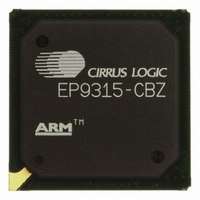
EP9315-CBZ Cirrus Logic Inc, EP9315-CBZ Datasheet - Page 500

EP9315-CBZ
Manufacturer Part Number
EP9315-CBZ
Description
IC ARM9 SOC ENH UNIV 352PBGA
Manufacturer
Cirrus Logic Inc
Series
EP9r
Specifications of EP9315-CBZ
Core Size
16/32-Bit
Core Processor
ARM9
Speed
200MHz
Connectivity
EBI/EMI, EIDE, Ethernet, I²C, IrDA, Keypad/Touchscreen, PCMCIA, SPI, UART/USART, USB
Peripherals
AC'97, DMA, I²:S, LCD, LED, MaverickKey, POR, PWM, WDT
Number Of I /o
16
Program Memory Type
ROMless
Ram Size
32K x 8
Voltage - Supply (vcc/vdd)
1.65 V ~ 3.6 V
Data Converters
A/D 8x12b
Oscillator Type
External
Operating Temperature
0°C ~ 70°C
Package / Case
352-BGA
Controller Family/series
(ARM9)
No. Of I/o's
16
Cpu Speed
200MHz
No. Of Timers
5
Digital Ic Case Style
BGA
Supply Voltage Range
1.65V To 1.94V, 3V To 3.6V
Embedded Interface Type
SPI
Rohs Compliant
Yes
Processor Series
EP93xx
Core
ARM920T
Data Bus Width
32 bit
3rd Party Development Tools
MDK-ARM, RL-ARM, ULINK2
Development Tools By Supplier
EDB9315A-Z
Case
BGA
Dc
06+
Lead Free Status / RoHS Status
Lead free / RoHS Compliant
For Use With
598-1144 - KIT DEVELOPMENT EP9315 ARM9
Eeprom Size
-
Program Memory Size
-
Lead Free Status / Rohs Status
Details
Other names
598-1139
Available stocks
Company
Part Number
Manufacturer
Quantity
Price
Part Number:
EP9315-CBZ
Manufacturer:
CIRRUS
Quantity:
20 000
- Current page: 500 of 824
- Download datasheet (13Mb)
13
13-4
SDRAM, SyncROM, and SyncFLASH Controller
EP93xx User’s Guide
SFLASH
13.4 SDRAM Initialization
2K Page
alike, 16
alike, 32
Device
SDRAM
SDRAM
512, 32
bit data
bit data
bit data
SROM
SROM
SROM
Sync
Mode,
16 bit
32 bit
32 bit
data
data
data
look
look
the synchronous memory map. Refer to
SROMLL=1 and SROMLL=0. bit can be used to reduce the number of memory segments
and it is
Following power on, each SDRAM device must be initialized before it can be used.
4
compatibility).
shows a general initialization sequence (refer to the SDRAM device’s data sheet to ensure
Address
Muxing
Row and
Row and
Row and
Row and
Row and
Row and
Column
Column
Column
Column
Column
Column
Pins
Bank
Bank
Bank
Bank
Bank
Bank
Step
1
Wait 100 μ s
A27
A27
A27
A27
A27
A27
A27
A27
A22
A22
A23
A23
AD
Address
15
Bank
Pins
1. “AP” means Auto Precharge -- see SDRAM device’s data sheet
A26
A26
A26
A26
A26
A26
A26
A26
A21
A21
A22
A22
AD
14
Table 13-3. Synchronous Memory Address Decoding
Table 13-4. General SDRAM Initialization Sequence
A22
A23
A24
A22
A27
A27
AD
13
-
-
-
-
-
-
Action
A21
A22
A23
A21
A26
A26
AD
12
-
-
-
-
-
-
Copyright 2007 Cirrus Logic
A20
A21
A22
A20
A20
A21
AD
11
-
-
-
-
-
-
A19
AP
A20
AP
A21
AP
A19
A19
AP
A20
AP
AD
10
-
1
1
1
1
1
Table 13-11
A18
A25
A19
A25
A20
A25
A18
A25
A18
A25
A19
A25
AD
9
A17
A24
A18
A24
A19
A10
A17
A24
A17
A24
A18
A24
AD
8
Address Pins
To allow SDRAM power and clocks to
stabilize
to compare the memory space with
A16
A17
A18
A16
A23
A16
A17
AD
A8
A9
A9
A8
A9
7
A15
A16
A17
A15
A15
A16
AD
A7
A8
A8
A8
A7
A8
6
Reason
A14
A15
A16
A14
A14
A15
AD
A6
A7
A7
A7
A6
A7
5
A13
A14
A15
A13
A13
A14
AD
A5
A6
A6
A6
A5
A6
4
A12
A13
A14
A12
A12
A13
AD
A4
A5
A5
A5
A4
A5
3
A12
A13
A12
A11
A11
A11
AD
A3
A4
A4
A4
A3
A4
2
DS785UM1
Table 13-
A10
A12
A10
A10
AD
A11
A11
A2
A3
A3
A3
A2
A3
1
A10
A10
AD
A11
A9
A1
A2
A2
A9
A2
A9
A1
A2
0
Related parts for EP9315-CBZ
Image
Part Number
Description
Manufacturer
Datasheet
Request
R

Part Number:
Description:
IC ARM920T MCU 200MHZ 352-PBGA
Manufacturer:
Cirrus Logic Inc
Datasheet:

Part Number:
Description:
32-Bit Microcontroller IC
Manufacturer:
Cirrus Logic Inc
Datasheet:

Part Number:
Description:
IC ARM920T MCU 200MHZ 352-PBGA
Manufacturer:
Cirrus Logic Inc
Datasheet:

Part Number:
Description:
MCU, MPU & DSP Development Tools Eval Bd Uni. ARM9 SOC Processor
Manufacturer:
Cirrus Logic Inc
Datasheet:

Part Number:
Description:
Development Kit
Manufacturer:
Cirrus Logic Inc
Datasheet:

Part Number:
Description:
Development Kit
Manufacturer:
Cirrus Logic Inc
Datasheet:

Part Number:
Description:
High-efficiency PFC + Fluorescent Lamp Driver Reference Design
Manufacturer:
Cirrus Logic Inc
Datasheet:

Part Number:
Description:
Development Kit
Manufacturer:
Cirrus Logic Inc
Datasheet:

Part Number:
Description:
Development Kit
Manufacturer:
Cirrus Logic Inc
Datasheet:

Part Number:
Description:
Development Kit
Manufacturer:
Cirrus Logic Inc
Datasheet:

Part Number:
Description:
Development Kit
Manufacturer:
Cirrus Logic Inc
Datasheet:

Part Number:
Description:
Development Kit
Manufacturer:
Cirrus Logic Inc
Datasheet:

Part Number:
Description:
Development Kit
Manufacturer:
Cirrus Logic Inc
Datasheet:

Part Number:
Description:
Ref Bd For Speakerbar MSA & DSP Products
Manufacturer:
Cirrus Logic Inc


