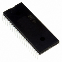
ST72F324J4B5 STMicroelectronics, ST72F324J4B5 Datasheet - Page 133

ST72F324J4B5
Manufacturer Part Number
ST72F324J4B5
Description
MCU 8BIT 16K FLASH 5V 42DIP
Manufacturer
STMicroelectronics
Series
ST7r
Datasheet
1.ST72F324J2T6.pdf
(164 pages)
Specifications of ST72F324J4B5
Core Processor
ST7
Core Size
8-Bit
Speed
8MHz
Connectivity
SCI, SPI
Peripherals
LVD, POR, PWM, WDT
Number Of I /o
32
Program Memory Size
16KB (16K x 8)
Program Memory Type
FLASH
Ram Size
512 x 8
Voltage - Supply (vcc/vdd)
3.8 V ~ 5.5 V
Data Converters
A/D 12x10b
Oscillator Type
Internal
Operating Temperature
-10°C ~ 85°C
Package / Case
42-DIP (0.600", 15.24mm)
Processor Series
ST72F3x
Core
ST7
Data Bus Width
8 bit
Data Ram Size
512 B
Interface Type
SCI, SPI
Maximum Clock Frequency
8 MHz
Number Of Programmable I/os
32
Number Of Timers
2
Maximum Operating Temperature
+ 85 C
Mounting Style
Through Hole
Development Tools By Supplier
ST7F521-IND/USB, ST7232X-EVAL, ST7MDT20-DVP3, ST7MDT20J-EMU3, STX-RLINK
Minimum Operating Temperature
- 10 C
On-chip Adc
10 bit, 12 Channel
For Use With
497-6421 - BOARD EVAL DGTL BATT CHGR DESIGN
Lead Free Status / RoHS Status
Lead free / RoHS Compliant
Eeprom Size
-
Lead Free Status / Rohs Status
Details
Other names
497-4848
Available stocks
Company
Part Number
Manufacturer
Quantity
Price
Company:
Part Number:
ST72F324J4B5
Manufacturer:
STMicroelectronics
Quantity:
135
12.9 I/O PORT PIN CHARACTERISTICS
12.9.1 General Characteristics
Subject to general operating conditions for V
Notes:
1. Data based on characterization results, not tested in production.
2. Hysteresis voltage between Schmitt trigger switching levels. Based on characterization results, not tested.
3. When the current limitation is not possible, the V
tion. A positive injection is induced by V
on page 117
4. Configuration not recommended, all unused pins must be kept at a fixed voltage: using the output mode of the I/O for
example and leaving the I/O unconnected on the board or an external pull-up or pull-down resistor (see
based on design simulation and/or technology characteristics, not tested in production.
5. The R
scribed in
6. To generate an external interrupt, a minimum pulse width has to be applied on an I/O port pin configured as an external
interrupt source.
Figure 69. Unused I/O Pins configured as input
ΣI
I
Symbol
INJ(PIN)
t
t
INJ(PIN)
Note: I/O can be left unconnected if it is configured as output
(0 or 1) by the software. This has the advantage of
t
greater EMC robustness and lower cost.
f(IO)out
r(IO)out
w(IT)in
V
R
C
V
V
I
lkg
I
hys
PU
S
IH
IO
IL
3)
PU
3)
Figure
Input low level voltage (standard voltage
devices)
Input high level voltage
Schmitt trigger voltage hysteresis
Injected Current on Flash device pin PB0
Injected Current on other I/O pins
Total injected current (sum of all I/O and
control pins)
Input leakage current
Static current consumption induced by each
floating input pin
Weak pull-up equivalent resistor
I/O pin capacitance
Output high to low level fall time
Output low to high level rise time
External interrupt pulse time
pull-up equivalent resistor is based on a resistive transistor (corresponding I
for more details.
70).
1)
V
DD
10kΩ
10kΩ
Parameter
UNUSED I/O PORT
UNUSED I/O PORT
1)
IN
6)
>V
ST7XXX
ST7XXX
DD
1)
5)
1)
2)
while a negative injection is induced by V
IN
DD
maximum must be respected, otherwise refer to I
, f
OSC
V
V
Floating input mode
V
C
Between 10% and
90%
DD
SS
IN
L
=50pF
=
, and T
=5V
Conditions
≤
V
Figure 70. Typical I
SS
V
IN
≤
V
A
V
DD
unless otherwise specified.
DD
9 0
8 0
7 0
6 0
5 0
4 0
3 0
2 0
1 0
=5V
0
2
4)
2 .5
0.7xV
T a = 1 4 0 ° C
T a = 9 5 ° C
T a = 2 5 ° C
T a = -4 5 ° C
3
Min
50
0
1
PU
3 .5
DD
ST72324Jx ST72324Kx
IN
V d d (V )
vs. V
<V
PU
4
SS
Typ
current characteristics de-
200
120
0.7
4 .5
25
25
5
. Refer to
DD
5
with V
5 .5
0.3xV
INJ(PIN)
Figure
Max
±25
250
+4
±4
±1
Section 12.2.2
6
IN
DD
=V
specifica-
69). Data
133/164
SS
Unit
t
mA
CPU
kΩ
µA
pF
ns
V
V
1


