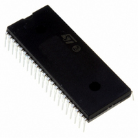
ST72F324J4B5 STMicroelectronics, ST72F324J4B5 Datasheet - Page 134

ST72F324J4B5
Manufacturer Part Number
ST72F324J4B5
Description
MCU 8BIT 16K FLASH 5V 42DIP
Manufacturer
STMicroelectronics
Series
ST7r
Datasheet
1.ST72F324J2T6.pdf
(164 pages)
Specifications of ST72F324J4B5
Core Processor
ST7
Core Size
8-Bit
Speed
8MHz
Connectivity
SCI, SPI
Peripherals
LVD, POR, PWM, WDT
Number Of I /o
32
Program Memory Size
16KB (16K x 8)
Program Memory Type
FLASH
Ram Size
512 x 8
Voltage - Supply (vcc/vdd)
3.8 V ~ 5.5 V
Data Converters
A/D 12x10b
Oscillator Type
Internal
Operating Temperature
-10°C ~ 85°C
Package / Case
42-DIP (0.600", 15.24mm)
Processor Series
ST72F3x
Core
ST7
Data Bus Width
8 bit
Data Ram Size
512 B
Interface Type
SCI, SPI
Maximum Clock Frequency
8 MHz
Number Of Programmable I/os
32
Number Of Timers
2
Maximum Operating Temperature
+ 85 C
Mounting Style
Through Hole
Development Tools By Supplier
ST7F521-IND/USB, ST7232X-EVAL, ST7MDT20-DVP3, ST7MDT20J-EMU3, STX-RLINK
Minimum Operating Temperature
- 10 C
On-chip Adc
10 bit, 12 Channel
For Use With
497-6421 - BOARD EVAL DGTL BATT CHGR DESIGN
Lead Free Status / RoHS Status
Lead free / RoHS Compliant
Eeprom Size
-
Lead Free Status / Rohs Status
Details
Other names
497-4848
Available stocks
Company
Part Number
Manufacturer
Quantity
Price
Company:
Part Number:
ST72F324J4B5
Manufacturer:
STMicroelectronics
Quantity:
135
ST72324Jx ST72324Kx
I/O PORT PIN CHARACTERISTICS (Cont’d)
12.9.2 Output Driving Current
Subject to general operating conditions for V
Figure 71. Typical V
Figure 72. Typ. V
Notes:
1. The I
(I/O ports and control pins) must not exceed I
2. The I
I
134/164
1
IO
Symbol
V
V
(I/O ports and control pins) must not exceed I
OH
OL
1 .2
0 .8
0 .6
0 .4
0 .2
0 .9
0 .8
0 .7
0 .6
0 .5
0 .4
0 .3
0 .2
0 .1
1)
2)
IO
IO
1
0
1
0
0
current sunk must always respect the absolute maximum rating specified in
current sourced must always respect the absolute maximum rating specified in
0
Output low level voltage for a standard I/O pin
when 8 pins are sunk at same time
(see
Output low level voltage for a high sink I/O pin
when 4 pins are sunk at same time
(see
Output high level voltage for an I/O pin
when 4 pins are sourced at same time
(see
10
Figure
Figure 72
Figure 73
OL
0.01
0 .0 0 5
5
at V
OL
71)
I
I
IO
IO
and
and
at V
20
DD
Ii o (A )
(mA)
(mA)
Iio (A )
Parameter
=5V (high-sink ports)
Figure
Figure
DD
0.0 2
=5V (std. ports)
Ta = 1 4 0 ° C "
Ta = 9 5 ° C
Ta = 2 5 ° C
Ta = -4 5 °C
0 .0 1
10
74)
76)
30
Ta = 1 4 0 °C
Ta = 9 5 °C
Ta = 2 5 °C
Ta = -4 5 ° C
VSS
0 .0 3
VDD
.
15
0 .0 1 5
DD
. True open drain I/O pins do not have V
, f
CPU
, and T
Figure 73. Typical V
I
I
I
I
I
I
IO
IO
IO
IO
IO
IO
5 .5
4 .5
3 .5
2 .5
A
Conditions
=+5mA
=+2mA
=+20mA, T
=+8mA
=-5mA, T
=-2mA
5
4
3
2
unless otherwise specified.
-0 .0 1
-10
T
T
A
A
A
A
-0 .0 0 8 -0 .0 0 6 -0 .0 0 4
≤85°C
>85°C
≤85°C
>85°C
-8
Section 12.2.2
OH
I
Section 12.2.2
-6
IO
V
V
V
at V
DD
DD
DD
(mA)
Ii o (A )
Min
OH
-1.4
-1.6
-0.7
DD
.
-4
V d d = 5 V 1 4 0 ° C m in
V d d = 5 v 9 5 °C m in
V d d = 5 v 2 5 °C m in
V d d = 5 v -4 5 °C m i n
=5V
and the sum of I
-0 .0 0 2
Max
-2
1.2
0.5
1.3
1.5
0.6
and the sum of
0
0
Unit
V
IO


