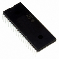
ST72F324J4B5 STMicroelectronics, ST72F324J4B5 Datasheet - Page 79

ST72F324J4B5
Manufacturer Part Number
ST72F324J4B5
Description
MCU 8BIT 16K FLASH 5V 42DIP
Manufacturer
STMicroelectronics
Series
ST7r
Datasheet
1.ST72F324J2T6.pdf
(164 pages)
Specifications of ST72F324J4B5
Core Processor
ST7
Core Size
8-Bit
Speed
8MHz
Connectivity
SCI, SPI
Peripherals
LVD, POR, PWM, WDT
Number Of I /o
32
Program Memory Size
16KB (16K x 8)
Program Memory Type
FLASH
Ram Size
512 x 8
Voltage - Supply (vcc/vdd)
3.8 V ~ 5.5 V
Data Converters
A/D 12x10b
Oscillator Type
Internal
Operating Temperature
-10°C ~ 85°C
Package / Case
42-DIP (0.600", 15.24mm)
Processor Series
ST72F3x
Core
ST7
Data Bus Width
8 bit
Data Ram Size
512 B
Interface Type
SCI, SPI
Maximum Clock Frequency
8 MHz
Number Of Programmable I/os
32
Number Of Timers
2
Maximum Operating Temperature
+ 85 C
Mounting Style
Through Hole
Development Tools By Supplier
ST7F521-IND/USB, ST7232X-EVAL, ST7MDT20-DVP3, ST7MDT20J-EMU3, STX-RLINK
Minimum Operating Temperature
- 10 C
On-chip Adc
10 bit, 12 Channel
For Use With
497-6421 - BOARD EVAL DGTL BATT CHGR DESIGN
Lead Free Status / RoHS Status
Lead free / RoHS Compliant
Eeprom Size
-
Lead Free Status / Rohs Status
Details
Other names
497-4848
Available stocks
Company
Part Number
Manufacturer
Quantity
Price
Company:
Part Number:
ST72F324J4B5
Manufacturer:
STMicroelectronics
Quantity:
135
10.4 SERIAL PERIPHERAL INTERFACE (SPI)
10.4.1 Introduction
The Serial Peripheral Interface (SPI) allows full-
duplex, synchronous, serial communication with
external devices. An SPI system may consist of a
master and one or more slaves however the SPI
interface can not be a master in a multi-master
system.
10.4.2 Main Features
■
■
■
■
■
■
■
■
■
Figure 46. Serial Peripheral Interface Block Diagram
Full duplex synchronous transfers (on 3 lines)
Simplex synchronous transfers (on 2 lines)
Master or slave operation
Six master mode frequencies (f
f
SS Management by software or hardware
Programmable clock polarity and phase
End of transfer interrupt flag
Write collision, Master Mode Fault and Overrun
flags
MOSI
MISO
CPU
SCK
SS
/2 max. slave mode frequency (see note)
SOD
bit
SPIDR
8-Bit Shift Register
Read Buffer
SERIAL CLOCK
CPU
GENERATOR
CONTROL
MASTER
/4 max.)
Data/Address Bus
Read
Write
Note: In slave mode, continuous transmission is
not possible at maximum frequency due to the
software overhead for clearing status flags and to
initiate the next transmission sequence.
10.4.3 General Description
Figure 46
(SPI) block diagram. There are 3 registers:
The SPI is connected to external devices through
4 pins:
– SPI Control Register (SPICR)
– SPI Control/Status Register (SPICSR)
– SPI Data Register (SPIDR)
– MISO: Master In / Slave Out data
– MOSI: Master Out / Slave In data
– SCK: Serial Clock out by SPI masters and in-
put by SPI slaves
7
SPIE
SPIF WCOL
7
SPE
shows the serial peripheral interface
CONTROL
SPR2
OVR
STATE
SPI
Interrupt
request
MODF
MSTR
ST72324Jx ST72324Kx
CPOL
0
CPHA
SOD
SS
SPICR
SPICSR
SSM
SPR1
0
1
SPR0
SSI
0
79/164
0
1


