MC56F8002VWL Freescale Semiconductor, MC56F8002VWL Datasheet - Page 19
MC56F8002VWL
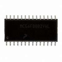
Manufacturer Part Number
MC56F8002VWL
Description
DSC 12K FLASH 32MHZ 28-SOIC
Manufacturer
Freescale Semiconductor
Series
56F8xxxr
Datasheet
1.MC56F8006DEMO.pdf
(100 pages)
Specifications of MC56F8002VWL
Core Processor
56800
Core Size
16-Bit
Speed
32MHz
Connectivity
I²C, LIN, SCI, SPI
Peripherals
LVD, POR, PWM, WDT
Number Of I /o
23
Program Memory Size
12KB (6K x 16)
Program Memory Type
FLASH
Ram Size
1K x 16
Voltage - Supply (vcc/vdd)
1.8 V ~ 3.6 V
Data Converters
A/D 15x12b
Oscillator Type
Internal
Operating Temperature
-40°C ~ 105°C
Package / Case
28-SOIC
Product
DSCs
Data Bus Width
16 bit
Processor Series
MC56F80xx
Core
56800E
Instruction Set Architecture
Dual Harvard
Device Million Instructions Per Second
32 MIPs
Maximum Clock Frequency
32 MHz
Number Of Programmable I/os
40
Data Ram Size
2 KB
Operating Supply Voltage
1.8 V to 3.6 V
Maximum Operating Temperature
+ 105 C
Mounting Style
SMD/SMT
Development Tools By Supplier
MC56F8006DEMO, APMOTOR56F8000E
Interface Type
LIN, I2C, SCI, SPI
Minimum Operating Temperature
- 40 C
For Use With
APMOTOR56F8000E - KIT DEMO MOTOR CTRL SYSTEM
Lead Free Status / RoHS Status
Lead free / RoHS Compliant
Eeprom Size
-
Lead Free Status / Rohs Status
Lead free / RoHS Compliant
Available stocks
Company
Part Number
Manufacturer
Quantity
Price

Part Number:
MC56F8002VWL
Manufacturer:
FREESCALE
Quantity:
20 000


Freescale Semiconductor
(CLKO_1)
(FAULT0)
(ANA1 &
(ANB13)
GPIOA6
GPIOB0
(PWM3)
(SCLK)
Signal
ANB1)
Name
(SCL)
(TXD)
(SCL)
(T1)
SOIC
28
12
15
LQFP
Table 5. 56F8006/56F8002 Signal and Package Information (continued)
32
18
21
LQFP
48
26
32
MC56F8006/MC56F8002 Digital Signal Controller, Rev. 3
Input/Open
Input/Open
Output
Analog
Output
Output
Output
Output
Output
Output
Analog
Output
Output
Input/
-drain
Input/
Input/
-drain
Input/
Type
Input
Input
Input
enabled
enabled
internal
internal
During
Reset
pullup
pullup
Input,
Input,
State
Port A GPIO — This GPIO pin can be individually programmed as
an input or output pin.
FAULT0 — PWM fault input 0 used for disabling selected PWM
outputs in cases where fault conditions originate off-chip.
ANA1 and ANB1 — Analog input to channel 1 of ADCA and ADCB.
SCL — The I
TXD — The SCI transmit data output or transmit/receive in single
wire operation.
CLKO_1 — This is a buffered clock output; the clock source is
selected by clockout select (CLKOSEL) bits in the clock output
select register (CLKOUT) in the SIM.
When used as an analog input, the signal goes to the ANA1 and
ANB1.
After reset, the default state is GPIOA6.
Port B GPIO — This GPIO pin can be individually programmed as
an input or output pin.
SCLK — The SPI serial clock. In master mode, this pin serves as
an output, clocking slaved listeners. In slave mode, this pin serves
as the data clock input.
SCL — The I
ANB13 — Analog input to channel 13 of ADCB
PWM3 — The PWM channel 3.
T1 — Dual timer module channel 1 input/output.
After reset, the default state is GPIOB0.
2
2
C serial clock
C serial clock.
Signal Description
Signal/Connection Descriptions
19
Related parts for MC56F8002VWL
Image
Part Number
Description
Manufacturer
Datasheet
Request
R

Part Number:
Description:
Manufacturer:
Freescale Semiconductor, Inc
Datasheet:
Part Number:
Description:
Manufacturer:
Freescale Semiconductor, Inc
Datasheet:
Part Number:
Description:
Manufacturer:
Freescale Semiconductor, Inc
Datasheet:
Part Number:
Description:
Manufacturer:
Freescale Semiconductor, Inc
Datasheet:
Part Number:
Description:
Manufacturer:
Freescale Semiconductor, Inc
Datasheet:
Part Number:
Description:
Manufacturer:
Freescale Semiconductor, Inc
Datasheet:
Part Number:
Description:
Manufacturer:
Freescale Semiconductor, Inc
Datasheet:
Part Number:
Description:
Manufacturer:
Freescale Semiconductor, Inc
Datasheet:
Part Number:
Description:
Manufacturer:
Freescale Semiconductor, Inc
Datasheet:
Part Number:
Description:
Manufacturer:
Freescale Semiconductor, Inc
Datasheet:
Part Number:
Description:
Manufacturer:
Freescale Semiconductor, Inc
Datasheet:
Part Number:
Description:
Manufacturer:
Freescale Semiconductor, Inc
Datasheet:
Part Number:
Description:
Manufacturer:
Freescale Semiconductor, Inc
Datasheet:
Part Number:
Description:
Manufacturer:
Freescale Semiconductor, Inc
Datasheet:
Part Number:
Description:
Manufacturer:
Freescale Semiconductor, Inc
Datasheet: