MC56F8002VWL Freescale Semiconductor, MC56F8002VWL Datasheet - Page 41
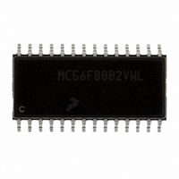
MC56F8002VWL
Manufacturer Part Number
MC56F8002VWL
Description
DSC 12K FLASH 32MHZ 28-SOIC
Manufacturer
Freescale Semiconductor
Series
56F8xxxr
Datasheet
1.MC56F8006DEMO.pdf
(100 pages)
Specifications of MC56F8002VWL
Core Processor
56800
Core Size
16-Bit
Speed
32MHz
Connectivity
I²C, LIN, SCI, SPI
Peripherals
LVD, POR, PWM, WDT
Number Of I /o
23
Program Memory Size
12KB (6K x 16)
Program Memory Type
FLASH
Ram Size
1K x 16
Voltage - Supply (vcc/vdd)
1.8 V ~ 3.6 V
Data Converters
A/D 15x12b
Oscillator Type
Internal
Operating Temperature
-40°C ~ 105°C
Package / Case
28-SOIC
Product
DSCs
Data Bus Width
16 bit
Processor Series
MC56F80xx
Core
56800E
Instruction Set Architecture
Dual Harvard
Device Million Instructions Per Second
32 MIPs
Maximum Clock Frequency
32 MHz
Number Of Programmable I/os
40
Data Ram Size
2 KB
Operating Supply Voltage
1.8 V to 3.6 V
Maximum Operating Temperature
+ 105 C
Mounting Style
SMD/SMT
Development Tools By Supplier
MC56F8006DEMO, APMOTOR56F8000E
Interface Type
LIN, I2C, SCI, SPI
Minimum Operating Temperature
- 40 C
For Use With
APMOTOR56F8000E - KIT DEMO MOTOR CTRL SYSTEM
Lead Free Status / RoHS Status
Lead free / RoHS Compliant
Eeprom Size
-
Lead Free Status / Rohs Status
Lead free / RoHS Compliant
Available stocks
Company
Part Number
Manufacturer
Quantity
Price

Part Number:
MC56F8002VWL
Manufacturer:
FREESCALE
Quantity:
20 000


8.2
Absolute maximum ratings are stress ratings only, and functional operation at the maxima is not guaranteed. Stress beyond the
limits specified
conditions, refer to the remaining tables in this section.
This device contains circuitry protecting against damage due to high static voltage or electrical fields; however, take normal
precautions to avoid application of any voltages higher than maximum-rated voltages to this high-impedance circuit. Reliability
of operation is enhanced if unused inputs are tied to an appropriate logic voltage level (for instance, either V
programmable pullup resistor associated with the pin is enabled.
1
2
3
8.2.1
Although damage from electrostatic discharge (ESD) is much less common on these devices than on early CMOS circuits, use
normal handling precautions to avoid exposure to static discharge. Qualification tests are performed to ensure that these devices
can withstand exposure to reasonable levels of static without suffering any permanent damage.
All ESD testing is in conformity with AEC-Q100 Stress Test Qualification for Automotive Grade Integrated Circuits. During
the device qualification ESD stresses were performed for the human body model (HBM), the machine model (MM), and the
charge device model (CDM).
Freescale Semiconductor
Output clamp current, per pin (V
Input must be current limited to the value specified. To determine the value of the required current-limiting resistor, calculate
resistance values for positive (V
All functional non-supply pins are internally clamped to V
Power supply must maintain regulation within operating VDD range during instantaneous and operating maximum current
conditions. If positive injection current (V
in external power supply going out of regulation. Ensure external V
current. This is the greatest risk when the MCU is not consuming power. Examples are: if no system clock is present or if the
clock rate is low (which would reduce overall power consumption).
Input clamp current, per pin (V
Voltage difference V
Voltage difference V
Analog Supply Voltage Range
Storage Temperature Range
Analog Input Voltage Range
Digital Input Voltage Range
(Normal Push-Pull mode)
Oscillator Voltage Range
Absolute Maximum Ratings
Supply Voltage Range
Output Voltage Range
Ambient Temperature
(Extended Industrial)
ESD Protection and Latch-Up Immunity
Table 12
Characteristic
Industrial
may affect device reliability or cause permanent damage to the device. For functional operating
DD
SS
to V
to V
IN
MC56F8006/MC56F8002 Digital Signal Controller, Rev. 3
DD
O
DDA
SSA
< 0)
< 0)
) and negative (V
1 2 3
1 2 3
Table 12. Absolute Maximum Ratings
In
> V
DD
) is greater than I
(V
Symbol
SS
SS
V
V
V
T
V
V
V
V
V
V
V
OSC
OUT
T
STG
DDA
INA
OC
) clamp voltages, then use the larger of the two resistance values.
DD
IN
IC
= 0 V, V
A
DD
SS
SS
and V
SSA
DD
DD
Pin Groups 1, 2
= 0 V)
DD
, the injection current may flow out of V
.
Pin Group 4
Pin Group 3
Pin Group 1
loads shunt current greater than maximum injection
Notes
–0.3
–0.3
–0.3
–0.3
–0.3
TBD
–0.3
–0.3
Min
–40
–55
—
—
V
–25.0
–20.0
DD
Max
TBD
V
105
150
3.8
3.6
0.3
0.3
3.6
DD
DD
+0.3
SS
and could result
Specifications
or V
DD
) or the
Unit
mA
mA
°C
°C
V
V
V
V
V
V
V
V
41
Related parts for MC56F8002VWL
Image
Part Number
Description
Manufacturer
Datasheet
Request
R

Part Number:
Description:
Manufacturer:
Freescale Semiconductor, Inc
Datasheet:
Part Number:
Description:
Manufacturer:
Freescale Semiconductor, Inc
Datasheet:
Part Number:
Description:
Manufacturer:
Freescale Semiconductor, Inc
Datasheet:
Part Number:
Description:
Manufacturer:
Freescale Semiconductor, Inc
Datasheet:
Part Number:
Description:
Manufacturer:
Freescale Semiconductor, Inc
Datasheet:
Part Number:
Description:
Manufacturer:
Freescale Semiconductor, Inc
Datasheet:
Part Number:
Description:
Manufacturer:
Freescale Semiconductor, Inc
Datasheet:
Part Number:
Description:
Manufacturer:
Freescale Semiconductor, Inc
Datasheet:
Part Number:
Description:
Manufacturer:
Freescale Semiconductor, Inc
Datasheet:
Part Number:
Description:
Manufacturer:
Freescale Semiconductor, Inc
Datasheet:
Part Number:
Description:
Manufacturer:
Freescale Semiconductor, Inc
Datasheet:
Part Number:
Description:
Manufacturer:
Freescale Semiconductor, Inc
Datasheet:
Part Number:
Description:
Manufacturer:
Freescale Semiconductor, Inc
Datasheet:
Part Number:
Description:
Manufacturer:
Freescale Semiconductor, Inc
Datasheet:
Part Number:
Description:
Manufacturer:
Freescale Semiconductor, Inc
Datasheet: