MC56F8002VWL Freescale Semiconductor, MC56F8002VWL Datasheet - Page 80
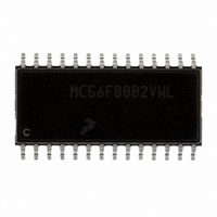
MC56F8002VWL
Manufacturer Part Number
MC56F8002VWL
Description
DSC 12K FLASH 32MHZ 28-SOIC
Manufacturer
Freescale Semiconductor
Series
56F8xxxr
Datasheet
1.MC56F8006DEMO.pdf
(100 pages)
Specifications of MC56F8002VWL
Core Processor
56800
Core Size
16-Bit
Speed
32MHz
Connectivity
I²C, LIN, SCI, SPI
Peripherals
LVD, POR, PWM, WDT
Number Of I /o
23
Program Memory Size
12KB (6K x 16)
Program Memory Type
FLASH
Ram Size
1K x 16
Voltage - Supply (vcc/vdd)
1.8 V ~ 3.6 V
Data Converters
A/D 15x12b
Oscillator Type
Internal
Operating Temperature
-40°C ~ 105°C
Package / Case
28-SOIC
Product
DSCs
Data Bus Width
16 bit
Processor Series
MC56F80xx
Core
56800E
Instruction Set Architecture
Dual Harvard
Device Million Instructions Per Second
32 MIPs
Maximum Clock Frequency
32 MHz
Number Of Programmable I/os
40
Data Ram Size
2 KB
Operating Supply Voltage
1.8 V to 3.6 V
Maximum Operating Temperature
+ 105 C
Mounting Style
SMD/SMT
Development Tools By Supplier
MC56F8006DEMO, APMOTOR56F8000E
Interface Type
LIN, I2C, SCI, SPI
Minimum Operating Temperature
- 40 C
For Use With
APMOTOR56F8000E - KIT DEMO MOTOR CTRL SYSTEM
Lead Free Status / RoHS Status
Lead free / RoHS Compliant
Eeprom Size
-
Lead Free Status / Rohs Status
Lead free / RoHS Compliant
Available stocks
Company
Part Number
Manufacturer
Quantity
Price

Part Number:
MC56F8002VWL
Manufacturer:
FREESCALE
Quantity:
20 000


Appendix B
Peripheral Register Memory Map and Reset Value
Offset
Addr.
(Hex)
00
01
02
03
Reset
Value
(Hex)
0000
0000
0000
0000
1
2
3
In
GPIOA_PUR is the same as GPIO_A_PUR).
Peripheral
Periph.
USER6
TMR0
TMR0
TMR0
TMR0
Two words are allocated for each entry in the vector table. This does not allow the full address range to be referenced from
the vector table, providing only 19 bits of address.
If the VBA is set to the reset value, the first two locations of the vector table overlay the chip reset addresses because the
reset address would match the base of this vector table.
USER6 vector can be defined as a fast interrupt if the instruction located in this vector location is not a JSR or BSR instruction.
Please see section 9.3.3.3 of DSP56800E 16-Bit Core Reference Manual for detail.
USER3
USER4
USER5
Table
42, ADC0 stands for ADCA, ADC1 stands for ADCB, and GPIOn is the same as GPIO_n (for example,
3
Register
COMP1
COMP2
TMR0_
TMR0_
TMR0_
TMR0_
CAPT
LOAD
Number
Vector
47
48
49
50
Table 41. Interrupt Vector Table Contents
Bit
15
Encoding
User
N/A
N/A
N/A
N/A
14
Table 42. Detailed Peripheral Memory Map
Priority
13
Level
1
2
2
2
12
Vector Base
Address +
P:0x5E
P:0x60
P:0x62
P:0x64
11
NOTE
10
1
9
User Programmable Priority Level 1 Interrupt
User Programmable Priority Level 2 Interrupt
User Programmable Priority Level 2 Interrupt
User Programmable Priority Level 2 Interrupt
COMPARISON_1
COMPARISON_2
CAPTURE
8
LOAD
7
Interrupt Function
6
5
4
3
2
1
Bit
0
Related parts for MC56F8002VWL
Image
Part Number
Description
Manufacturer
Datasheet
Request
R

Part Number:
Description:
Manufacturer:
Freescale Semiconductor, Inc
Datasheet:
Part Number:
Description:
Manufacturer:
Freescale Semiconductor, Inc
Datasheet:
Part Number:
Description:
Manufacturer:
Freescale Semiconductor, Inc
Datasheet:
Part Number:
Description:
Manufacturer:
Freescale Semiconductor, Inc
Datasheet:
Part Number:
Description:
Manufacturer:
Freescale Semiconductor, Inc
Datasheet:
Part Number:
Description:
Manufacturer:
Freescale Semiconductor, Inc
Datasheet:
Part Number:
Description:
Manufacturer:
Freescale Semiconductor, Inc
Datasheet:
Part Number:
Description:
Manufacturer:
Freescale Semiconductor, Inc
Datasheet:
Part Number:
Description:
Manufacturer:
Freescale Semiconductor, Inc
Datasheet:
Part Number:
Description:
Manufacturer:
Freescale Semiconductor, Inc
Datasheet:
Part Number:
Description:
Manufacturer:
Freescale Semiconductor, Inc
Datasheet:
Part Number:
Description:
Manufacturer:
Freescale Semiconductor, Inc
Datasheet:
Part Number:
Description:
Manufacturer:
Freescale Semiconductor, Inc
Datasheet:
Part Number:
Description:
Manufacturer:
Freescale Semiconductor, Inc
Datasheet:
Part Number:
Description:
Manufacturer:
Freescale Semiconductor, Inc
Datasheet: