MC56F8002VWL Freescale Semiconductor, MC56F8002VWL Datasheet - Page 29
MC56F8002VWL
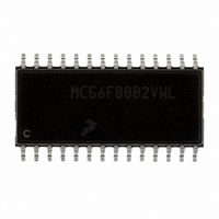
Manufacturer Part Number
MC56F8002VWL
Description
DSC 12K FLASH 32MHZ 28-SOIC
Manufacturer
Freescale Semiconductor
Series
56F8xxxr
Datasheet
1.MC56F8006DEMO.pdf
(100 pages)
Specifications of MC56F8002VWL
Core Processor
56800
Core Size
16-Bit
Speed
32MHz
Connectivity
I²C, LIN, SCI, SPI
Peripherals
LVD, POR, PWM, WDT
Number Of I /o
23
Program Memory Size
12KB (6K x 16)
Program Memory Type
FLASH
Ram Size
1K x 16
Voltage - Supply (vcc/vdd)
1.8 V ~ 3.6 V
Data Converters
A/D 15x12b
Oscillator Type
Internal
Operating Temperature
-40°C ~ 105°C
Package / Case
28-SOIC
Product
DSCs
Data Bus Width
16 bit
Processor Series
MC56F80xx
Core
56800E
Instruction Set Architecture
Dual Harvard
Device Million Instructions Per Second
32 MIPs
Maximum Clock Frequency
32 MHz
Number Of Programmable I/os
40
Data Ram Size
2 KB
Operating Supply Voltage
1.8 V to 3.6 V
Maximum Operating Temperature
+ 105 C
Mounting Style
SMD/SMT
Development Tools By Supplier
MC56F8006DEMO, APMOTOR56F8000E
Interface Type
LIN, I2C, SCI, SPI
Minimum Operating Temperature
- 40 C
For Use With
APMOTOR56F8000E - KIT DEMO MOTOR CTRL SYSTEM
Lead Free Status / RoHS Status
Lead free / RoHS Compliant
Eeprom Size
-
Lead Free Status / Rohs Status
Lead free / RoHS Compliant
Available stocks
Company
Part Number
Manufacturer
Quantity
Price

Part Number:
MC56F8002VWL
Manufacturer:
FREESCALE
Quantity:
20 000


5.3
The 56F8006/56F8002 series contain a dual access memory. It can be accessed from core primary data buses (XAB1; CDBW;
CDBR) and secondary data buses (XAB2; XDB2). Addresses in data memory are selected on the XAB1 and XAB2 buses. Byte,
word, and long data transfers occur on the 32-bit CDBR and CDBW buses. A second 16-bit read operation can be performed
in parallel on the XDB2 bus.
Peripheral registers and on-chip JTAG/EOnCE controller registers are memory-mapped into data memory access. A special
direct address mode is supported for accessing a first 64-location in data memory by using a single word instruction.
The data memory map is shown in
Freescale Semiconductor
1
2
All addresses are 16-bit word addresses.
This RAM is shared with data space starting at address X: 0x00 0000; see
Data Map
Begin/End Address
P: 0x1F FFFF
P: 0x00 83FF
P: 0x00 7FFF
P: 0x00 1FFF
P: 0x00 07FF
P: 0x00 8800
P: 0x00 8000
P: 0x00 2000
P: 0x00 0800
P: 0x00 0000
1
2
All addresses are 16-bit word addresses.
This RAM is shared with Program space starting at P: 0x00 8000. See
Figure
Table 8. Program Memory Map
Begin/End Address
8.
X:0xFF FFFF
X:0xFF FEFF
X:0xFF FF00
X:0x00 FFFF
X:0x00 EFFF
X:0x00 87FF
X:0x00 7FFF
X:0x00 03FF
X:0x01 0000
X:0x00 F000
X:0x00 8800
X:0x00 8000
X:0x00 0400
X:0x00 0000
MC56F8006/MC56F8002 Digital Signal Controller, Rev. 3
Table
RESERVED
On-Chip RAM
RESERVED
RESERVED
• Internal program flash: 12 KB
• Interrupt vector table locates from 0x00 0800 to 0x00 0865
• COP reset address = 0x00 0802
• Boot location = 0x00 0800
9.
Table 9. Data Memory Map
2
: 2 KB
1
for 56F8002 at Reset (continued)
Memory Allocation
4096 locations allocated
256 locations allocated
Memory Allocation
On-Chip Peripherals
On-Chip Data RAM
RESERVED
RESERVED
RESERVED
RESERVED
EOnCE
1
2 KB
2
Figure
Figure 7
8.
and
Memory Maps
29
Related parts for MC56F8002VWL
Image
Part Number
Description
Manufacturer
Datasheet
Request
R

Part Number:
Description:
Manufacturer:
Freescale Semiconductor, Inc
Datasheet:
Part Number:
Description:
Manufacturer:
Freescale Semiconductor, Inc
Datasheet:
Part Number:
Description:
Manufacturer:
Freescale Semiconductor, Inc
Datasheet:
Part Number:
Description:
Manufacturer:
Freescale Semiconductor, Inc
Datasheet:
Part Number:
Description:
Manufacturer:
Freescale Semiconductor, Inc
Datasheet:
Part Number:
Description:
Manufacturer:
Freescale Semiconductor, Inc
Datasheet:
Part Number:
Description:
Manufacturer:
Freescale Semiconductor, Inc
Datasheet:
Part Number:
Description:
Manufacturer:
Freescale Semiconductor, Inc
Datasheet:
Part Number:
Description:
Manufacturer:
Freescale Semiconductor, Inc
Datasheet:
Part Number:
Description:
Manufacturer:
Freescale Semiconductor, Inc
Datasheet:
Part Number:
Description:
Manufacturer:
Freescale Semiconductor, Inc
Datasheet:
Part Number:
Description:
Manufacturer:
Freescale Semiconductor, Inc
Datasheet:
Part Number:
Description:
Manufacturer:
Freescale Semiconductor, Inc
Datasheet:
Part Number:
Description:
Manufacturer:
Freescale Semiconductor, Inc
Datasheet:
Part Number:
Description:
Manufacturer:
Freescale Semiconductor, Inc
Datasheet: