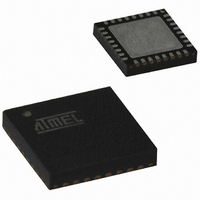
AT89C5131A-PUTUM Atmel, AT89C5131A-PUTUM Datasheet - Page 105

AT89C5131A-PUTUM
Manufacturer Part Number
AT89C5131A-PUTUM
Description
IC 8051 MCU FLASH 32K USB 32QFN
Manufacturer
Atmel
Series
AT89C513xr
Datasheet
1.AT89C5130A-PUTUM.pdf
(188 pages)
Specifications of AT89C5131A-PUTUM
Core Processor
C52X2
Core Size
8-Bit
Speed
48MHz
Connectivity
I²C, SPI, UART/USART, USB
Peripherals
LED, POR, PWM, WDT
Number Of I /o
18
Program Memory Size
32KB (32K x 8)
Program Memory Type
FLASH
Eeprom Size
4K x 8
Ram Size
1.25K x 8
Voltage - Supply (vcc/vdd)
2.7 V ~ 5.5 V
Oscillator Type
Internal
Operating Temperature
-40°C ~ 85°C
Package / Case
32-VQFN Exposed Pad, 32-HVQFN, 32-SQFN, 32-DHVQFN
Core
8051
Processor Series
AT89x
Data Bus Width
8 bit
Maximum Clock Frequency
48 MHz
Data Ram Size
1.25 KB
Number Of Programmable I/os
34
Number Of Timers
16 bit
Operating Supply Voltage
2.7 V to 5.5 V
Mounting Style
SMD/SMT
Height
0.95 mm
Interface Type
2-Wire, EUART, SPI, USB
Length
7 mm
Maximum Operating Temperature
+ 85 C
Minimum Operating Temperature
- 40 C
Supply Voltage (max)
5.5 V
Supply Voltage (min)
2.7 V
Width
7 mm
For Use With
AT89OCD-01 - USB EMULATOR FOR AT8XC51 MCUAT89STK-10 - KIT EVAL APPL MASS STORAGEAT89STK-05 - KIT STARTER FOR AT89C5131
Lead Free Status / RoHS Status
Lead free / RoHS Compliant
Data Converters
-
Lead Free Status / Rohs Status
Details
Available stocks
Company
Part Number
Manufacturer
Quantity
Price
Part Number:
AT89C5131A-PUTUM
Manufacturer:
ATMEL/爱特梅尔
Quantity:
20 000
20.1.1
20.1.2
4337K–USB–04/08
Master Transmitter Mode
Master Receiver Mode
R
W
A:
A: Not acknowledge bit (high level at SDA)
Data: 8-bit data byte
P
In Figure 20-4 to Figure 20-7, circles are used to indicate when the serial interrupt flag is set.
The numbers in the circles show the status code held in SSCS. At these points, a service routine
must be executed to continue or complete the serial transfer. These service routines are not crit-
ical since the serial transfer is suspended until the serial interrupt flag is cleared by software.
When the serial interrupt routine is entered, the status code in SSCS is used to branch to the
appropriate service routine. For each status code, the required software action and details of the
following serial transfer are given in Table to Table 20-9.
In the master transmitter mode, a number of data bytes are transmitted to a slave receiver
(Figure 20-4). Before the master transmitter mode can be entered, SSCON must be initialised as
follows:
Table 20-1.
CR0, CR1 and CR2 define the internal serial bit rate if external bit rate generator is not used.
SSIE must be set to enable TWI. STA, STO and SI must be cleared.
The master transmitter mode may now be entered by setting the STA bit. The 2-wire logic will
now test the 2-wire bus and generate a START condition as soon as the bus becomes free.
When a START condition is transmitted, the serial interrupt flag (SI bit in SSCON) is set, and the
status code in SSCS will be 08h. This status must be used to vector to an interrupt routine that
loads SSDAT with the slave address and the data direction bit (SLA+W).
When the slave address and the direction bit have been transmitted and an acknowledgement
bit has been received, SI is set again and a number of status code in SSCS are possible. There
are 18h, 20h or 38h for the master mode and also 68h, 78h or B0h if the slave mode was
enabled (AA=logic 1). The appropriate action to be taken for each of these status code is
detailed in Table . This scheme is repeated until a STOP condition is transmitted.
SSIE, CR2, CR1 and CR0 are not affected by the serial transfer and are referred to Table 7 to
Table 11. After a repeated START condition (state 10h) the TWI module may switch to the mas-
ter receiver mode by loading SSDAT with SLA+R.
In the master receiver mode, a number of data bytes are received from a slave transmitter
(Figure 20-5). The transfer is initialized as in the master transmitter mode. When the START
condition has been transmitted, the interrupt routine must load SSDAT with the 7-bit slave
bit rate
CR2
: Read bit (high level at SDA)
: Write bit (low level at SDA)
Acknowledge bit (low level at SDA)
: STOP condition
SSCON Initialization
SSIE
1
STA
0
STO
0
SI
0
AT89C5130A/31A-M
AA
X
bit rate
CR1
bit rate
CR0
105


