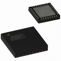
AT89C5131A-PUTUM Atmel, AT89C5131A-PUTUM Datasheet - Page 97

AT89C5131A-PUTUM
Manufacturer Part Number
AT89C5131A-PUTUM
Description
IC 8051 MCU FLASH 32K USB 32QFN
Manufacturer
Atmel
Series
AT89C513xr
Datasheet
1.AT89C5130A-PUTUM.pdf
(188 pages)
Specifications of AT89C5131A-PUTUM
Core Processor
C52X2
Core Size
8-Bit
Speed
48MHz
Connectivity
I²C, SPI, UART/USART, USB
Peripherals
LED, POR, PWM, WDT
Number Of I /o
18
Program Memory Size
32KB (32K x 8)
Program Memory Type
FLASH
Eeprom Size
4K x 8
Ram Size
1.25K x 8
Voltage - Supply (vcc/vdd)
2.7 V ~ 5.5 V
Oscillator Type
Internal
Operating Temperature
-40°C ~ 85°C
Package / Case
32-VQFN Exposed Pad, 32-HVQFN, 32-SQFN, 32-DHVQFN
Core
8051
Processor Series
AT89x
Data Bus Width
8 bit
Maximum Clock Frequency
48 MHz
Data Ram Size
1.25 KB
Number Of Programmable I/os
34
Number Of Timers
16 bit
Operating Supply Voltage
2.7 V to 5.5 V
Mounting Style
SMD/SMT
Height
0.95 mm
Interface Type
2-Wire, EUART, SPI, USB
Length
7 mm
Maximum Operating Temperature
+ 85 C
Minimum Operating Temperature
- 40 C
Supply Voltage (max)
5.5 V
Supply Voltage (min)
2.7 V
Width
7 mm
For Use With
AT89OCD-01 - USB EMULATOR FOR AT8XC51 MCUAT89STK-10 - KIT EVAL APPL MASS STORAGEAT89STK-05 - KIT STARTER FOR AT89C5131
Lead Free Status / RoHS Status
Lead free / RoHS Compliant
Data Converters
-
Lead Free Status / Rohs Status
Details
Available stocks
Company
Part Number
Manufacturer
Quantity
Price
Part Number:
AT89C5131A-PUTUM
Manufacturer:
ATMEL/爱特梅尔
Quantity:
20 000
- Current page: 97 of 188
- Download datasheet (2Mb)
Figure 19-4. Data Transmission Format (CPHA = 0)
Figure 19-5. Data Transmission Format (CPHA = 1)
Figure 19-6. CPHA/SS Timing
4337K–USB–04/08
MOSI (from Master)
SCK cycle number
MISO (from Slave)
MOSI (from Master)
SCK (CPOL = 0)
SCK (CPOL = 1)
MISO (from Slave)
SCK cycle number
SPEN (internal)
SCK (CPOL = 0)
SCK (CPOL = 1)
Capture point
SPEN (internal)
SS (to Slave)
Capture point
SS (to Slave)
output data are shifted (Figure 19-4 and Figure 19-5). The clock phase and polarity should be
identical for the Master SPI device and the communicating Slave device.
As shown in
must begin driving its data before the first SCK edge, and a falling edge on the SS pin is used to
start the transmission. The SS pin must be toggled high and then low between each byte trans-
mitted (Figure 19-2).
Figure 19-6
ing its MOSI pin on the first SCK edge. Therefore the Slave uses the first SCK edge as a start
transmission signal. The SS pin can remain low between transmissions
mat may be preferable in systems having only one Master and only one Slave driving the MISO
data line.
MISO/MOSI
(CPHA = 0)
(CPHA = 1)
Master SS
Slave SS
Slave SS
shows an SPI transmission in which CPHA is’1’. In this case, the Master begins driv-
Figure
MSB
MSB
MSB
1
MSB
1
19-5, the first SCK edge is the MSB capture strobe. Therefore the Slave
2
bit6
bit6
2
bit6
Byte 1
bit6
3
bit5
bit5
3
bit5
bit5
bit4
4
bit4
bit4
4
bit4
Byte 2
bit3
bit3
5
bit3
bit3
5
6
bit2
bit2
6
bit2
bit2
Byte 3
7
bit1
bit1
7
bit1
AT89C5130A/31A-M
bit1
LSB
8
LSB
LSB
8
LSB
(Figure
19-1). This for-
97
Related parts for AT89C5131A-PUTUM
Image
Part Number
Description
Manufacturer
Datasheet
Request
R

Part Number:
Description:
Manufacturer:
Atmel Corporation
Datasheet:

Part Number:
Description:
Manufacturer:
Atmel Corporation
Datasheet:

Part Number:
Description:
IC 8051 MCU FLASH 32K USB 52PLCC
Manufacturer:
Atmel
Datasheet:

Part Number:
Description:
IC MCU 32KB 3-3.6V USB 48-VQFN
Manufacturer:
Atmel
Datasheet:

Part Number:
Description:
MCU 8051 32K FLASH USB 28-SOIC
Manufacturer:
Atmel
Datasheet:

Part Number:
Description:
IC 8051 MCU FLASH 32K USB 64VQFP
Manufacturer:
Atmel
Datasheet:

Part Number:
Description:
MCU 8051 32K FLASH USB 64-VQFP
Manufacturer:
Atmel
Datasheet:

Part Number:
Description:
MCU 8051 32K FLASH USB 28-SOIC
Manufacturer:
Atmel
Datasheet:

Part Number:
Description:
MCU 8051 32K FLASH USB 52-PLCC
Manufacturer:
Atmel
Datasheet:

Part Number:
Description:
IC 8051 MCU FLASH 32K USB 48QFN
Manufacturer:
Atmel
Datasheet:

Part Number:
Description:
IC 8051 MCU FLASH 32K USB 64VQFP
Manufacturer:
Atmel
Datasheet:

Part Number:
Description:
IC 8051 MCU FLASH 32K USB 32QFN
Manufacturer:
Atmel
Datasheet:

Part Number:
Description:
IC 8051 MCU FLASH 32K USB 52PLCC
Manufacturer:
Atmel
Datasheet:

Part Number:
Description:
IC 8051 MCU FLASH 32K USB 28SOIC
Manufacturer:
Atmel
Datasheet:


