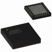
AT89C5131A-PUTUM Atmel, AT89C5131A-PUTUM Datasheet - Page 93

AT89C5131A-PUTUM
Manufacturer Part Number
AT89C5131A-PUTUM
Description
IC 8051 MCU FLASH 32K USB 32QFN
Manufacturer
Atmel
Series
AT89C513xr
Datasheet
1.AT89C5130A-PUTUM.pdf
(188 pages)
Specifications of AT89C5131A-PUTUM
Core Processor
C52X2
Core Size
8-Bit
Speed
48MHz
Connectivity
I²C, SPI, UART/USART, USB
Peripherals
LED, POR, PWM, WDT
Number Of I /o
18
Program Memory Size
32KB (32K x 8)
Program Memory Type
FLASH
Eeprom Size
4K x 8
Ram Size
1.25K x 8
Voltage - Supply (vcc/vdd)
2.7 V ~ 5.5 V
Oscillator Type
Internal
Operating Temperature
-40°C ~ 85°C
Package / Case
32-VQFN Exposed Pad, 32-HVQFN, 32-SQFN, 32-DHVQFN
Core
8051
Processor Series
AT89x
Data Bus Width
8 bit
Maximum Clock Frequency
48 MHz
Data Ram Size
1.25 KB
Number Of Programmable I/os
34
Number Of Timers
16 bit
Operating Supply Voltage
2.7 V to 5.5 V
Mounting Style
SMD/SMT
Height
0.95 mm
Interface Type
2-Wire, EUART, SPI, USB
Length
7 mm
Maximum Operating Temperature
+ 85 C
Minimum Operating Temperature
- 40 C
Supply Voltage (max)
5.5 V
Supply Voltage (min)
2.7 V
Width
7 mm
For Use With
AT89OCD-01 - USB EMULATOR FOR AT8XC51 MCUAT89STK-10 - KIT EVAL APPL MASS STORAGEAT89STK-05 - KIT STARTER FOR AT89C5131
Lead Free Status / RoHS Status
Lead free / RoHS Compliant
Data Converters
-
Lead Free Status / Rohs Status
Details
Available stocks
Company
Part Number
Manufacturer
Quantity
Price
Part Number:
AT89C5131A-PUTUM
Manufacturer:
ATMEL/爱特梅尔
Quantity:
20 000
19. Serial Peripheral Interface (SPI)
19.1
19.2
19.2.1
19.2.2
4337K–USB–04/08
Features
Signal Description
Master Output Slave Input (MOSI)
Master Input Slave Output (MISO)
The Serial Peripheral Interface module (SPI) allows full-duplex, synchronous, serial communica-
tion between the MCU and peripheral devices, including other MCUs.
Features of the SPI module include the following:
Figure 19-1
peripherals. The bus is made of three wires connecting all the devices:
Figure 19-1. SPI Master/Slaves Interconnection
The Master device selects the individual Slave devices by using four pins of a parallel port to
control the four SS pins of the Slave devices.
This 1-bit signal is directly connected between the Master Device and a Slave Device. The MOSI
line is used to transfer data in series from the Master to the Slave. Therefore, it is an output sig-
nal from the Master, and an input signal to a Slave. A byte (8-bit word) is transmitted most
significant bit (MSB) first, least significant bit (LSB) last.
This 1-bit signal is directly connected between the Slave Device and a Master Device. The MISO
line is used to transfer data in series from the Slave to the Master. Therefore, it is an output sig-
nal from the Slave, and an input signal to the Master. A byte (8-bit word) is transmitted most
significant bit (MSB) first, least significant bit (LSB) last.
• Full-duplex, three-wire synchronous transfers
• Master or Slave operation
• Eight programmable Master clock rates
• Serial clock with programmable polarity and phase
• Master mode fault error flag with MCU interrupt capability
• Write collision flag protection
shows a typical SPI bus configuration using one Master controller and many Slave
Master
Slave 4
MISO
MOSI
SCK
SS
0
1
2
3
VDD
Slave 3
AT89C5130A/31A-M
Slave 1
Slave 2
93


