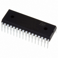
ST72F63BK4B1 STMicroelectronics, ST72F63BK4B1 Datasheet - Page 127

ST72F63BK4B1
Manufacturer Part Number
ST72F63BK4B1
Description
IC MCU 8BIT 16K FLASH 32-SDIP
Manufacturer
STMicroelectronics
Series
ST7r
Datasheet
1.ST72F63BD6U1TR.pdf
(186 pages)
Specifications of ST72F63BK4B1
Core Processor
ST7
Core Size
8-Bit
Speed
8MHz
Connectivity
I²C, SCI, USB
Peripherals
DMA, LVD, POR, PWM, WDT
Number Of I /o
19
Program Memory Size
16KB (16K x 8)
Program Memory Type
FLASH
Ram Size
512 x 8
Voltage - Supply (vcc/vdd)
4 V ~ 5.5 V
Data Converters
A/D 12x8b
Oscillator Type
External
Operating Temperature
0°C ~ 70°C
Package / Case
32-SDIP (0.400", 10.16mm)
Processor Series
ST72F6x
Core
ST7
Data Bus Width
8 bit
Data Ram Size
512 B
Interface Type
I2C, SCI
Maximum Clock Frequency
8 MHz
Number Of Programmable I/os
19
Number Of Timers
1
Maximum Operating Temperature
+ 70 C
Mounting Style
Through Hole
Development Tools By Supplier
ST7MDTU3-EPB/US, ST72F63B-SK/RAIS, ST7MDTU3-EMU3, STX-RLINK
Minimum Operating Temperature
0 C
On-chip Adc
8 bit, 8 Channel / 8 bit, 12 Channel
For Use With
497-5521 - EVAL BOARD LOW SPEED USB
Lead Free Status / RoHS Status
Lead free / RoHS Compliant
Eeprom Size
-
Lead Free Status / Rohs Status
Details
- Current page: 127 of 186
- Download datasheet (3Mb)
ST7263Bxx
11.6.4
Note:
Software procedure
Refer to the control/status register (CSR) and data register (DR) in
definitions and to
ADC configuration
The total duration of the A/D conversion is 12 ADC clock periods (1/f
The analog input ports must be configured as input, no pull-up, no interrupt. Refer to the
«I/O ports» chapter. Using these pins as analog inputs does not affect the ability of the port
to be read as a logic input.
In the CSR register:
●
ADC conversion
In the CSR register:
●
When a conversion is complete:
●
●
●
A write to the CSR register (with ADON set) aborts the current conversion, resets the COCO
bit and starts a new conversion.
Figure 51. ADC conversion timings
Low power modes
Table 44.
The A/D converter may be disabled by resetting the ADON bit. This feature allows reduced
power consumption when no conversion is needed and between single shot conversions.
WAIT
HALT
Select the CH[3:0] bits to assign the analog channel to be converted.
Set the ADON bit to enable the A/D converter and to start the first conversion. From this
time on, the ADC performs a continuous conversion of the selected channel.
The COCO bit is set by hardware.
No interrupt is generated.
The result is in the DR register and remains valid until the next conversion has ended.
Mode
Low power modes
Figure 51
A/D Converter disabled.
After wakeup from Halt mode, the A/D Converter requires a stabilization time
before accurate conversions can be performed.
No effect on A/D Converter
ADON
HOLD
CONTROL
t
LOAD
for the timings.
Doc ID 7516 Rev 8
t
CONV
COCO BIT SET
ADCCSR WRITE
OPERATION
Description
Section 11.6.6
ADC
On-chip peripherals
=4/f
CPU
).
for the bit
127/186
Related parts for ST72F63BK4B1
Image
Part Number
Description
Manufacturer
Datasheet
Request
R

Part Number:
Description:
KIT STARTER LOW COST ST7
Manufacturer:
STMicroelectronics
Datasheet:

Part Number:
Description:
LOW SPEED USB 8-BIT MCU FAMILY WITH FLASH/ROM, UP TO 512 BYTES RAM, 8-BIT ADC, WDG, TIMER, SCI & I�C
Manufacturer:
STMICROELECTRONICS [STMicroelectronics]
Datasheet:

Part Number:
Description:
STMicroelectronics [RIPPLE-CARRY BINARY COUNTER/DIVIDERS]
Manufacturer:
STMicroelectronics
Datasheet:

Part Number:
Description:
STMicroelectronics [LIQUID-CRYSTAL DISPLAY DRIVERS]
Manufacturer:
STMicroelectronics
Datasheet:

Part Number:
Description:
BOARD EVAL FOR MEMS SENSORS
Manufacturer:
STMicroelectronics
Datasheet:

Part Number:
Description:
NPN TRANSISTOR POWER MODULE
Manufacturer:
STMicroelectronics
Datasheet:

Part Number:
Description:
TURBOSWITCH ULTRA-FAST HIGH VOLTAGE DIODE
Manufacturer:
STMicroelectronics
Datasheet:

Part Number:
Description:
Manufacturer:
STMicroelectronics
Datasheet:

Part Number:
Description:
DIODE / SCR MODULE
Manufacturer:
STMicroelectronics
Datasheet:

Part Number:
Description:
DIODE / SCR MODULE
Manufacturer:
STMicroelectronics
Datasheet:

Part Number:
Description:
Search -----> STE16N100
Manufacturer:
STMicroelectronics
Datasheet:

Part Number:
Description:
Search ---> STE53NA50
Manufacturer:
STMicroelectronics
Datasheet:


