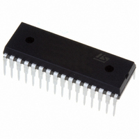
ST72F63BK4B1 STMicroelectronics, ST72F63BK4B1 Datasheet - Page 156

ST72F63BK4B1
Manufacturer Part Number
ST72F63BK4B1
Description
IC MCU 8BIT 16K FLASH 32-SDIP
Manufacturer
STMicroelectronics
Series
ST7r
Datasheet
1.ST72F63BD6U1TR.pdf
(186 pages)
Specifications of ST72F63BK4B1
Core Processor
ST7
Core Size
8-Bit
Speed
8MHz
Connectivity
I²C, SCI, USB
Peripherals
DMA, LVD, POR, PWM, WDT
Number Of I /o
19
Program Memory Size
16KB (16K x 8)
Program Memory Type
FLASH
Ram Size
512 x 8
Voltage - Supply (vcc/vdd)
4 V ~ 5.5 V
Data Converters
A/D 12x8b
Oscillator Type
External
Operating Temperature
0°C ~ 70°C
Package / Case
32-SDIP (0.400", 10.16mm)
Processor Series
ST72F6x
Core
ST7
Data Bus Width
8 bit
Data Ram Size
512 B
Interface Type
I2C, SCI
Maximum Clock Frequency
8 MHz
Number Of Programmable I/os
19
Number Of Timers
1
Maximum Operating Temperature
+ 70 C
Mounting Style
Through Hole
Development Tools By Supplier
ST7MDTU3-EPB/US, ST72F63B-SK/RAIS, ST7MDTU3-EMU3, STX-RLINK
Minimum Operating Temperature
0 C
On-chip Adc
8 bit, 8 Channel / 8 bit, 12 Channel
For Use With
497-5521 - EVAL BOARD LOW SPEED USB
Lead Free Status / RoHS Status
Lead free / RoHS Compliant
Eeprom Size
-
Lead Free Status / Rohs Status
Details
- Current page: 156 of 186
- Download datasheet (3Mb)
Electrical characteristics
13.9
Table 72.
1. Hysteresis voltage between Schmitt trigger switching levels. Based on characterization results, not tested.
2. The I
3. The R
4. To guarantee the reset of the device, a minimum pulse has to be applied to RESET pin. All short pulses applied on RESET
156/186
t
w(RSTL)out
t
Symbol
h(RSTL)in
ports and control pins) must not exceed I
tested in production.
pin with a duration below t
R
V
V
V
V
hys
OL
ON
IH
IL
IO
ON
current sunk must always respect the absolute maximum rating specified in
pull-up equivalent resistor is based on a resistive transistor. This data is based on characterization results, not
Input high level voltage
Input low voltage
Schmitt trigger voltage
hysteresis
Output low level voltage
Weak pull-up equivalent resistor
(3)
Generated reset pulse duration
External reset pulse hold time
Figure 72. |V
Control pin characteristics
Subject to general operating conditions for V
Asynchronous RESET pin
(1)
Parameter
h(RSTL)in
DD
0.9
0.8
0.7
0.6
0.5
0.4
0.3
0.2
0.1
-V
can be ignored.
0
OH
(2)
4
| @ I
VSS
(4)
.
IO
4.2
=10 mA (high current)
V
V
External pin or
internal reset sources
DD
IN
Doc ID 7516 Rev 8
=
=5 V
V
4.4
SS
Conditions
|Vdd - Voh| (V) at Iio=-10mA
I
I
V
IO
IO
DD
4.6
=5 mA
=7.5 mA
=5 V
DD
Vdd (V)
, f
CPU
4.8
, and T
0.7xV
V
Min
50
5
5
SS
-
-
-
-
Section 13.2
DD
A
unless otherwise specified.
5.2
Typ
400
80
30
6
-
-
-
-
-
and the sum of I
5.4
ai17706
-
-
0.3xV
Max
V
100
0.8
1.3
DD
D
-
D
ST7263Bxx
IO
1/f
Unit
(I/O
SFOSC
mV
kΩ
µs
µs
V
V
V
Related parts for ST72F63BK4B1
Image
Part Number
Description
Manufacturer
Datasheet
Request
R

Part Number:
Description:
KIT STARTER LOW COST ST7
Manufacturer:
STMicroelectronics
Datasheet:

Part Number:
Description:
LOW SPEED USB 8-BIT MCU FAMILY WITH FLASH/ROM, UP TO 512 BYTES RAM, 8-BIT ADC, WDG, TIMER, SCI & I�C
Manufacturer:
STMICROELECTRONICS [STMicroelectronics]
Datasheet:

Part Number:
Description:
STMicroelectronics [RIPPLE-CARRY BINARY COUNTER/DIVIDERS]
Manufacturer:
STMicroelectronics
Datasheet:

Part Number:
Description:
STMicroelectronics [LIQUID-CRYSTAL DISPLAY DRIVERS]
Manufacturer:
STMicroelectronics
Datasheet:

Part Number:
Description:
BOARD EVAL FOR MEMS SENSORS
Manufacturer:
STMicroelectronics
Datasheet:

Part Number:
Description:
NPN TRANSISTOR POWER MODULE
Manufacturer:
STMicroelectronics
Datasheet:

Part Number:
Description:
TURBOSWITCH ULTRA-FAST HIGH VOLTAGE DIODE
Manufacturer:
STMicroelectronics
Datasheet:

Part Number:
Description:
Manufacturer:
STMicroelectronics
Datasheet:

Part Number:
Description:
DIODE / SCR MODULE
Manufacturer:
STMicroelectronics
Datasheet:

Part Number:
Description:
DIODE / SCR MODULE
Manufacturer:
STMicroelectronics
Datasheet:

Part Number:
Description:
Search -----> STE16N100
Manufacturer:
STMicroelectronics
Datasheet:

Part Number:
Description:
Search ---> STE53NA50
Manufacturer:
STMicroelectronics
Datasheet:


