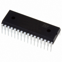
ST72F63BK4B1 STMicroelectronics, ST72F63BK4B1 Datasheet - Page 140

ST72F63BK4B1
Manufacturer Part Number
ST72F63BK4B1
Description
IC MCU 8BIT 16K FLASH 32-SDIP
Manufacturer
STMicroelectronics
Series
ST7r
Datasheet
1.ST72F63BD6U1TR.pdf
(186 pages)
Specifications of ST72F63BK4B1
Core Processor
ST7
Core Size
8-Bit
Speed
8MHz
Connectivity
I²C, SCI, USB
Peripherals
DMA, LVD, POR, PWM, WDT
Number Of I /o
19
Program Memory Size
16KB (16K x 8)
Program Memory Type
FLASH
Ram Size
512 x 8
Voltage - Supply (vcc/vdd)
4 V ~ 5.5 V
Data Converters
A/D 12x8b
Oscillator Type
External
Operating Temperature
0°C ~ 70°C
Package / Case
32-SDIP (0.400", 10.16mm)
Processor Series
ST72F6x
Core
ST7
Data Bus Width
8 bit
Data Ram Size
512 B
Interface Type
I2C, SCI
Maximum Clock Frequency
8 MHz
Number Of Programmable I/os
19
Number Of Timers
1
Maximum Operating Temperature
+ 70 C
Mounting Style
Through Hole
Development Tools By Supplier
ST7MDTU3-EPB/US, ST72F63B-SK/RAIS, ST7MDTU3-EMU3, STX-RLINK
Minimum Operating Temperature
0 C
On-chip Adc
8 bit, 8 Channel / 8 bit, 12 Channel
For Use With
497-5521 - EVAL BOARD LOW SPEED USB
Lead Free Status / RoHS Status
Lead free / RoHS Compliant
Eeprom Size
-
Lead Free Status / Rohs Status
Details
- Current page: 140 of 186
- Download datasheet (3Mb)
Electrical characteristics
140/186
Table 56.
1. All power (V
2. I
3. Negative injection disturbs the analog performance of the device. In particular, it induces leakage currents
4. When several inputs are submitted to a current injection, the maximum
5. True open drain I/O port pins do not accept positive injection.
Table 57.
cannot be respected, the injection current must be limited externally to the I
injection is induced by V
there is no positive injection current, and the corresponding V
throughout the device including the analog inputs. To avoid undesirable effects on the analog functions,
care must be taken:
- Analog input pins must have a negative injection less than 0.8 mA (assuming that the impedance of the
analog voltage is lower than the specified limits)
- Pure digital pins must have a negative injection less than 1.6mA. In addition, it is recommended to inject
the current as far as possible from the analog input pins.
positive and negative injected currents (instantaneous values). These results are based on
characterization with
INJ(PIN)
I
I
ΣI
INJ(PIN)
INJ(PIN)
Symbol
Symbol
INJ(PIN)
T
I
I
VDD
VSS
I
STG
T
IO
must never be exceeded. This is implicitly insured if V
J
(2)(3)
(2)(3)
(2)
Current characteristics
Thermal characteristics
DD
) and ground (V
Total current into V
Total current out of V
Output current sunk by any standard I/O and
control pin
Output current sunk by any high sink I/O pin
Output current source by any I/Os and control
pin
Injected current on V
Injected current on RESET pin
Injected current on OSCIN and OSCOUT pins
Injected current on any other pin
Total injected current (sum of all I/O and
control pins)
Negative injected current to PB0 (10 mA)/AIN0
pin
Storage temperature range
Maximum junction temperature
Σ
I
INJ(PIN)
IN
>V
DD
SS
maximum current injection on four I/O port pins of the device.
while a negative injection is induced by V
) lines must be connected to the external supply.
(4)
Doc ID 7516 Rev 8
DD
Ratings
Ratings
SS
PP
power lines (source)
ground lines (sink)
pin
(4)(5)
IN
IN
maximum must always be respected.
maximum is respected. If V
(1)
(1)
Σ
I
IN
INJ(PIN)
<V
INJ(PIN)
See
characteristics
SS
Maximum value
. For true open-drain pads,
-65 to +150
is the absolute sum of the
Section 14.2:
Thermal
value. A positive
T
Value
± 20
- 25
- 80
± 5
± 5
± 5
± 5
Jmax
80
80
25
50
IN
for
maximum
ST7263Bxx
Unit
Unit
mA
°C
µA
Related parts for ST72F63BK4B1
Image
Part Number
Description
Manufacturer
Datasheet
Request
R

Part Number:
Description:
KIT STARTER LOW COST ST7
Manufacturer:
STMicroelectronics
Datasheet:

Part Number:
Description:
LOW SPEED USB 8-BIT MCU FAMILY WITH FLASH/ROM, UP TO 512 BYTES RAM, 8-BIT ADC, WDG, TIMER, SCI & I�C
Manufacturer:
STMICROELECTRONICS [STMicroelectronics]
Datasheet:

Part Number:
Description:
STMicroelectronics [RIPPLE-CARRY BINARY COUNTER/DIVIDERS]
Manufacturer:
STMicroelectronics
Datasheet:

Part Number:
Description:
STMicroelectronics [LIQUID-CRYSTAL DISPLAY DRIVERS]
Manufacturer:
STMicroelectronics
Datasheet:

Part Number:
Description:
BOARD EVAL FOR MEMS SENSORS
Manufacturer:
STMicroelectronics
Datasheet:

Part Number:
Description:
NPN TRANSISTOR POWER MODULE
Manufacturer:
STMicroelectronics
Datasheet:

Part Number:
Description:
TURBOSWITCH ULTRA-FAST HIGH VOLTAGE DIODE
Manufacturer:
STMicroelectronics
Datasheet:

Part Number:
Description:
Manufacturer:
STMicroelectronics
Datasheet:

Part Number:
Description:
DIODE / SCR MODULE
Manufacturer:
STMicroelectronics
Datasheet:

Part Number:
Description:
DIODE / SCR MODULE
Manufacturer:
STMicroelectronics
Datasheet:

Part Number:
Description:
Search -----> STE16N100
Manufacturer:
STMicroelectronics
Datasheet:

Part Number:
Description:
Search ---> STE53NA50
Manufacturer:
STMicroelectronics
Datasheet:


