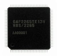
DF2265TE13V Renesas Electronics America, DF2265TE13V Datasheet - Page 102

DF2265TE13V
Manufacturer Part Number
DF2265TE13V
Description
IC H8S/2265 MCU FLASH 100TQFP
Manufacturer
Renesas Electronics America
Series
H8® H8S/2200r
Specifications of DF2265TE13V
Core Processor
H8S/2000
Core Size
16-Bit
Speed
13MHz
Connectivity
I²C, SCI, SmartCard
Peripherals
LCD, POR, PWM, WDT
Number Of I /o
67
Program Memory Size
128KB (128K x 8)
Program Memory Type
FLASH
Ram Size
4K x 8
Voltage - Supply (vcc/vdd)
3 V ~ 5.5 V
Data Converters
A/D 10x10b, D/A 2x8b
Oscillator Type
Internal
Operating Temperature
-20°C ~ 75°C
Package / Case
100-TQFP, 100-VQFP
Lead Free Status / RoHS Status
Lead free / RoHS Compliant
Eeprom Size
-
Available stocks
Company
Part Number
Manufacturer
Quantity
Price
Company:
Part Number:
DF2265TE13V
Manufacturer:
Renesas Electronics America
Quantity:
10 000
- Current page: 102 of 712
- Download datasheet (5Mb)
Section 2 CPU
The BSET, BCLR, BNOT, BST and BIST instructions are executed as follows:
1. Data is read in bytes.
2. The operation corresponding to the instruction is applied to the specified bit of the data.
3. The byte produced by the bit-manipulation is written back.
• Consider this example, where the BCLR instruction is executed to clear only bit 4 in P1DDR
Rev. 5.00 Sep. 01, 2009 Page 50 of 656
REJ09B0071-0500
I/O
P1DDR
I/O
P1DDR
Read value
of Port 1.
P1DDR is an 8-bit register that consists of write-only bits and specifies input or output for
each pin of port 1. Reading of these bits is not valid, since values read are specified as
undefined.
In the following example, the BCLR instruction specifies P14 as an input. Before the
operation, P17 to P14 are set as output pins and P13 to P10 are set as input pins. The value of
P1DDR is H'F0.
To switch P14 from an output to an input, the value of bit 4 in P1DDR has to be changed from
1 to 0 (H'F0 to H'E0). The BCLR instruction used to clear bit 4 in P1DDR is as follows.
BCLR
However, the above bit-manipulation of the write-only P1DDR register may cause the
following problem.
The data in P1DDR is read in bytes. Data read from P1DDR is undefined. Thus, regardless of
whether the value in the register is 0 or 1, it is impossible to tell which value will be read. All
bits in P1DDR are write-only, thus read as undefined. The actual value in P1DDR is H'F0. Let
us assume that the value read is H'F8, where the value of bit 3 is read as 1 rather than its actual
value of 0.
#4, @P1DDR
Output
Output
P17
P17
1
1
1
Output
Output
P16
P16
1
1
1
Output
Output
P15
P15
1
1
1
Output
Output
P14
P14
1
1
1
Input
Input
P13
P13
0
0
1
Input
Input
P12
P12
0
0
0
Input
Input
P11
P11
0
0
0
Input
Input
P10
P10
0
0
0
Related parts for DF2265TE13V
Image
Part Number
Description
Manufacturer
Datasheet
Request
R

Part Number:
Description:
CONN SOCKET 2POS 7.92MM WHITE
Manufacturer:
Hirose Electric Co Ltd
Datasheet:

Part Number:
Description:
CONN SOCKET 4POS 7.92MM WHITE
Manufacturer:
Hirose Electric Co Ltd
Datasheet:

Part Number:
Description:
CONN SOCKET 5POS 7.92MM WHITE
Manufacturer:
Hirose Electric Co Ltd
Datasheet:

Part Number:
Description:
CONN SOCKET 3POS 7.92MM WHITE
Manufacturer:
Hirose Electric Co Ltd
Datasheet:

Part Number:
Description:
CONN SOCKET 5POS 7.92MM WHITE
Manufacturer:
Hirose Electric Co Ltd
Datasheet:

Part Number:
Description:
CONN SOCKET 2POS 7.92MM WHITE
Manufacturer:
Hirose Electric Co Ltd
Datasheet:

Part Number:
Description:
CONN SOCKET 3POS 7.92MM WHITE
Manufacturer:
Hirose Electric Co Ltd
Datasheet:

Part Number:
Description:
CONN SOCKET 4POS 7.92MM WHITE
Manufacturer:
Hirose Electric Co Ltd
Datasheet:

Part Number:
Description:
CONN HEADER 2POS 7.92MM R/A TIN
Manufacturer:
Hirose Electric Co Ltd
Datasheet:

Part Number:
Description:
CONN HEADER 4POS 7.92MM R/A TIN
Manufacturer:
Hirose Electric Co Ltd
Datasheet:

Part Number:
Description:
KIT STARTER FOR M16C/29
Manufacturer:
Renesas Electronics America
Datasheet:

Part Number:
Description:
KIT STARTER FOR R8C/2D
Manufacturer:
Renesas Electronics America
Datasheet:

Part Number:
Description:
R0K33062P STARTER KIT
Manufacturer:
Renesas Electronics America
Datasheet:

Part Number:
Description:
KIT STARTER FOR R8C/23 E8A
Manufacturer:
Renesas Electronics America
Datasheet:

Part Number:
Description:
KIT STARTER FOR R8C/25
Manufacturer:
Renesas Electronics America
Datasheet:


