DF2265TE13V Renesas Electronics America, DF2265TE13V Datasheet - Page 5
DF2265TE13V
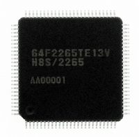
Manufacturer Part Number
DF2265TE13V
Description
IC H8S/2265 MCU FLASH 100TQFP
Manufacturer
Renesas Electronics America
Series
H8® H8S/2200r
Specifications of DF2265TE13V
Core Processor
H8S/2000
Core Size
16-Bit
Speed
13MHz
Connectivity
I²C, SCI, SmartCard
Peripherals
LCD, POR, PWM, WDT
Number Of I /o
67
Program Memory Size
128KB (128K x 8)
Program Memory Type
FLASH
Ram Size
4K x 8
Voltage - Supply (vcc/vdd)
3 V ~ 5.5 V
Data Converters
A/D 10x10b, D/A 2x8b
Oscillator Type
Internal
Operating Temperature
-20°C ~ 75°C
Package / Case
100-TQFP, 100-VQFP
Lead Free Status / RoHS Status
Lead free / RoHS Compliant
Eeprom Size
-
Available stocks
Company
Part Number
Manufacturer
Quantity
Price
Company:

Part Number:
DF2265TE13V
Manufacturer:
Renesas Electronics America
Quantity:
10 000


General Precautions in the Handling of MPU/MCU Products
The following usage notes are applicable to all MPU/MCU products from Renesas. For detailed usage notes
on the products covered by this manual, refer to the relevant sections of the manual. If the descriptions under
General Precautions in the Handling of MPU/MCU Products and in the body of the manual differ from each
other, the description in the body of the manual takes precedence.
1. Handling of Unused Pins
2. Processing at Power-on
3. Prohibition of Access to Reserved Addresses
4. Clock Signals
5. Differences between Products
Handle unused pins in accord with the directions given under Handling of Unused Pins in
the manual.
⎯ The input pins of CMOS products are generally in the high-impedance state. In
The state of the product is undefined at the moment when power is supplied.
⎯ The states of internal circuits in the LSI are indeterminate and the states of register
Access to reserved addresses is prohibited.
⎯ The reserved addresses are provided for the possible future expansion of functions. Do
After applying a reset, only release the reset line after the operating clock signal has
become stable. When switching the clock signal during program execution, wait until the
target clock signal has stabilized.
⎯ When the clock signal is generated with an external resonator (or from an external
Before changing from one product to another, i.e. to one with a different type number,
confirm that the change will not lead to problems.
⎯
operation with an unused pin in the open-circuit state, extra electromagnetic noise is
induced in the vicinity of LSI, an associated shoot-through current flows internally, and
malfunctions may occur due to the false recognition of the pin state as an input signal.
Unused pins should be handled as described under Handling of Unused Pins in the
manual.
settings and pins are undefined at the moment when power is supplied.
In a finished product where the reset signal is applied to the external reset pin, the
states of pins are not guaranteed from the moment when power is supplied until the
reset process is completed.
In a similar way, the states of pins in a product that is reset by an on-chip power-on
reset function are not guaranteed from the moment when power is supplied until the
power reaches the level at which resetting has been specified.
not access these addresses; the correct operation of LSI is not guaranteed if they are
accessed.
oscillator) during a reset, ensure that the reset line is only released after full stabilization
of the clock signal. Moreover, when switching to a clock signal produced with an
external resonator (or by an external oscillator) while program execution is in progress,
wait until the target clock signal is stable.
The characteristics of MPU/MCU in the same group but having different type numbers
may differ because of the differences in internal memory capacity and layout pattern.
When changing to products of different type numbers, implement a system-evaluation
test for each of the products.
Rev. 5.00 Sep. 01, 2009 Page iii of l
REJ09B0071-0500
Related parts for DF2265TE13V
Image
Part Number
Description
Manufacturer
Datasheet
Request
R

Part Number:
Description:
CONN SOCKET 2POS 7.92MM WHITE
Manufacturer:
Hirose Electric Co Ltd
Datasheet:

Part Number:
Description:
CONN SOCKET 4POS 7.92MM WHITE
Manufacturer:
Hirose Electric Co Ltd
Datasheet:

Part Number:
Description:
CONN SOCKET 5POS 7.92MM WHITE
Manufacturer:
Hirose Electric Co Ltd
Datasheet:

Part Number:
Description:
CONN SOCKET 3POS 7.92MM WHITE
Manufacturer:
Hirose Electric Co Ltd
Datasheet:
Part Number:
Description:
CONN SOCKET 5POS 7.92MM WHITE
Manufacturer:
Hirose Electric Co Ltd
Datasheet:

Part Number:
Description:
CONN SOCKET 2POS 7.92MM WHITE
Manufacturer:
Hirose Electric Co Ltd
Datasheet:
Part Number:
Description:
CONN SOCKET 3POS 7.92MM WHITE
Manufacturer:
Hirose Electric Co Ltd
Datasheet:
Part Number:
Description:
CONN SOCKET 4POS 7.92MM WHITE
Manufacturer:
Hirose Electric Co Ltd
Datasheet:

Part Number:
Description:
CONN HEADER 2POS 7.92MM R/A TIN
Manufacturer:
Hirose Electric Co Ltd
Datasheet:

Part Number:
Description:
CONN HEADER 4POS 7.92MM R/A TIN
Manufacturer:
Hirose Electric Co Ltd
Datasheet:

Part Number:
Description:
KIT STARTER FOR M16C/29
Manufacturer:
Renesas Electronics America
Datasheet:

Part Number:
Description:
KIT STARTER FOR R8C/2D
Manufacturer:
Renesas Electronics America
Datasheet:

Part Number:
Description:
R0K33062P STARTER KIT
Manufacturer:
Renesas Electronics America
Datasheet:

Part Number:
Description:
KIT STARTER FOR R8C/23 E8A
Manufacturer:
Renesas Electronics America
Datasheet:

Part Number:
Description:
KIT STARTER FOR R8C/25
Manufacturer:
Renesas Electronics America
Datasheet: