DF2265TE13V Renesas Electronics America, DF2265TE13V Datasheet - Page 203
DF2265TE13V
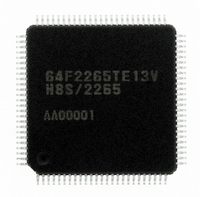
Manufacturer Part Number
DF2265TE13V
Description
IC H8S/2265 MCU FLASH 100TQFP
Manufacturer
Renesas Electronics America
Series
H8® H8S/2200r
Specifications of DF2265TE13V
Core Processor
H8S/2000
Core Size
16-Bit
Speed
13MHz
Connectivity
I²C, SCI, SmartCard
Peripherals
LCD, POR, PWM, WDT
Number Of I /o
67
Program Memory Size
128KB (128K x 8)
Program Memory Type
FLASH
Ram Size
4K x 8
Voltage - Supply (vcc/vdd)
3 V ~ 5.5 V
Data Converters
A/D 10x10b, D/A 2x8b
Oscillator Type
Internal
Operating Temperature
-20°C ~ 75°C
Package / Case
100-TQFP, 100-VQFP
Lead Free Status / RoHS Status
Lead free / RoHS Compliant
Eeprom Size
-
Available stocks
Company
Part Number
Manufacturer
Quantity
Price
Company:

Part Number:
DF2265TE13V
Manufacturer:
Renesas Electronics America
Quantity:
10 000


• P10/TIOCA0 *
Notes: 1. In the H8S/2268 Group, this pin functions as TIOCA0 input when TPU channel 0 timer
9.2
Port 3 is a 6-bit I/O port. The P34, P35, and SCK1 function as NMOS push-pull outputs. Port 3
has the following registers.
• Port 3 data direction register (P3DDR)
• Port 3 data register (P3DR)
• Port 3 register (PORT3)
• Port 3 open drain control register (P3ODR)
9.2.1
P3DDR specifies input or output of the port 3 pins using the individual bits.
P3DDR cannot be read; if it is, an undefined value will be read.
The value of this register when read is undefined after a bit manipulation instruction is executed.
To prevent undefined read values, do not use bit manipulation instructions to write to this register.
For details, see section 2.9.4, Access Methods for Registers with Write-Only Bits.
TPU Channel 0 Setting *
P10DDR
Pin function
The pin function is switched as shown below according to the combination of the TPU channel
0 *
2
setting and the P10DDR bit.
2. Supported only by the H8S/2268 Group.
Port 3
Port 3 Data Direction Register (P3DDR)
operating mode is set to normal operation and IOA3 to IOA0 in TIORH_0 are set to
10xx.
2
2
TIOCA0 output *
Output
⎯
2
Rev. 5.00 Sep. 01, 2009 Page 151 of 656
P10 input
0
Input or Initial Value
TIOCA0 input *
Section 9 I/O Ports
REJ09B0071-0500
P10 output
1
*
2
1
Related parts for DF2265TE13V
Image
Part Number
Description
Manufacturer
Datasheet
Request
R

Part Number:
Description:
CONN SOCKET 2POS 7.92MM WHITE
Manufacturer:
Hirose Electric Co Ltd
Datasheet:

Part Number:
Description:
CONN SOCKET 4POS 7.92MM WHITE
Manufacturer:
Hirose Electric Co Ltd
Datasheet:

Part Number:
Description:
CONN SOCKET 5POS 7.92MM WHITE
Manufacturer:
Hirose Electric Co Ltd
Datasheet:

Part Number:
Description:
CONN SOCKET 3POS 7.92MM WHITE
Manufacturer:
Hirose Electric Co Ltd
Datasheet:
Part Number:
Description:
CONN SOCKET 5POS 7.92MM WHITE
Manufacturer:
Hirose Electric Co Ltd
Datasheet:

Part Number:
Description:
CONN SOCKET 2POS 7.92MM WHITE
Manufacturer:
Hirose Electric Co Ltd
Datasheet:
Part Number:
Description:
CONN SOCKET 3POS 7.92MM WHITE
Manufacturer:
Hirose Electric Co Ltd
Datasheet:
Part Number:
Description:
CONN SOCKET 4POS 7.92MM WHITE
Manufacturer:
Hirose Electric Co Ltd
Datasheet:

Part Number:
Description:
CONN HEADER 2POS 7.92MM R/A TIN
Manufacturer:
Hirose Electric Co Ltd
Datasheet:

Part Number:
Description:
CONN HEADER 4POS 7.92MM R/A TIN
Manufacturer:
Hirose Electric Co Ltd
Datasheet:

Part Number:
Description:
KIT STARTER FOR M16C/29
Manufacturer:
Renesas Electronics America
Datasheet:

Part Number:
Description:
KIT STARTER FOR R8C/2D
Manufacturer:
Renesas Electronics America
Datasheet:

Part Number:
Description:
R0K33062P STARTER KIT
Manufacturer:
Renesas Electronics America
Datasheet:

Part Number:
Description:
KIT STARTER FOR R8C/23 E8A
Manufacturer:
Renesas Electronics America
Datasheet:

Part Number:
Description:
KIT STARTER FOR R8C/25
Manufacturer:
Renesas Electronics America
Datasheet: