DF2265TE13V Renesas Electronics America, DF2265TE13V Datasheet - Page 189
DF2265TE13V
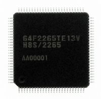
Manufacturer Part Number
DF2265TE13V
Description
IC H8S/2265 MCU FLASH 100TQFP
Manufacturer
Renesas Electronics America
Series
H8® H8S/2200r
Specifications of DF2265TE13V
Core Processor
H8S/2000
Core Size
16-Bit
Speed
13MHz
Connectivity
I²C, SCI, SmartCard
Peripherals
LCD, POR, PWM, WDT
Number Of I /o
67
Program Memory Size
128KB (128K x 8)
Program Memory Type
FLASH
Ram Size
4K x 8
Voltage - Supply (vcc/vdd)
3 V ~ 5.5 V
Data Converters
A/D 10x10b, D/A 2x8b
Oscillator Type
Internal
Operating Temperature
-20°C ~ 75°C
Package / Case
100-TQFP, 100-VQFP
Lead Free Status / RoHS Status
Lead free / RoHS Compliant
Eeprom Size
-
Available stocks
Company
Part Number
Manufacturer
Quantity
Price
Company:

Part Number:
DF2265TE13V
Manufacturer:
Renesas Electronics America
Quantity:
10 000


4.
5.
6.
7.
8.8
8.8.1
DTC operation can be disabled or enabled using the module stop control register. The initial
setting is for DTC operation to be enabled. Register access is disabled by setting module stop
mode. Module stop mode cannot be set during DTC operation. For details, refer to section 22,
Power-Down Modes.
8.8.2
The MRA, MRB, SAR, DAR, CRA, and CRB registers are all located in on-chip RAM. When the
DTC bit is used, the RAME bit in SYSCR should not be cleared to 0.
8.8.3
For DTCE bit setting, use bit manipulation instructions such as BSET and BCLR. If all interrupts
are masked, multiple activation sources can be set at one time (only at the initial setting) by
writing data after executing a dummy read on the relevant register.
Write 1 to the SWDTE bit and the vector number (H'60) to DTVECR. The write data is
H'E0.
Read DTVECR again and check that it is set to the vector number (H'60). If it is not, this
indicates that the write failed. This is presumably because an interrupt occurred between steps
3 and 4 and led to a different software activation. To activate this transfer, go back to step 3.
If the write was successful, the DTC is activated and a block of 128 bytes of data is
transferred.
After the transfer, an SWDTEND interrupt occurs. The interrupt handling routine should
clear the SWDTE bit to 0 and perform other wrap-up processing.
Usage Notes
Module Stop Mode Setting
On-Chip RAM
DTCE Bit Setting
Rev. 5.00 Sep. 01, 2009 Page 137 of 656
Section 8 Data Transfer Controller (DTC)
REJ09B0071-0500
Related parts for DF2265TE13V
Image
Part Number
Description
Manufacturer
Datasheet
Request
R

Part Number:
Description:
CONN SOCKET 2POS 7.92MM WHITE
Manufacturer:
Hirose Electric Co Ltd
Datasheet:

Part Number:
Description:
CONN SOCKET 4POS 7.92MM WHITE
Manufacturer:
Hirose Electric Co Ltd
Datasheet:

Part Number:
Description:
CONN SOCKET 5POS 7.92MM WHITE
Manufacturer:
Hirose Electric Co Ltd
Datasheet:

Part Number:
Description:
CONN SOCKET 3POS 7.92MM WHITE
Manufacturer:
Hirose Electric Co Ltd
Datasheet:
Part Number:
Description:
CONN SOCKET 5POS 7.92MM WHITE
Manufacturer:
Hirose Electric Co Ltd
Datasheet:

Part Number:
Description:
CONN SOCKET 2POS 7.92MM WHITE
Manufacturer:
Hirose Electric Co Ltd
Datasheet:
Part Number:
Description:
CONN SOCKET 3POS 7.92MM WHITE
Manufacturer:
Hirose Electric Co Ltd
Datasheet:
Part Number:
Description:
CONN SOCKET 4POS 7.92MM WHITE
Manufacturer:
Hirose Electric Co Ltd
Datasheet:

Part Number:
Description:
CONN HEADER 2POS 7.92MM R/A TIN
Manufacturer:
Hirose Electric Co Ltd
Datasheet:

Part Number:
Description:
CONN HEADER 4POS 7.92MM R/A TIN
Manufacturer:
Hirose Electric Co Ltd
Datasheet:

Part Number:
Description:
KIT STARTER FOR M16C/29
Manufacturer:
Renesas Electronics America
Datasheet:

Part Number:
Description:
KIT STARTER FOR R8C/2D
Manufacturer:
Renesas Electronics America
Datasheet:

Part Number:
Description:
R0K33062P STARTER KIT
Manufacturer:
Renesas Electronics America
Datasheet:

Part Number:
Description:
KIT STARTER FOR R8C/23 E8A
Manufacturer:
Renesas Electronics America
Datasheet:

Part Number:
Description:
KIT STARTER FOR R8C/25
Manufacturer:
Renesas Electronics America
Datasheet: