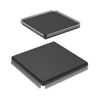
HD6417727F100V Renesas Electronics America, HD6417727F100V Datasheet - Page 16

HD6417727F100V
Manufacturer Part Number
HD6417727F100V
Description
MPU 3V 16K PB-FREE 240-QFP
Manufacturer
Renesas Electronics America
Series
SuperH® SH7700r
Datasheet
1.HD6417727BP100CV.pdf
(1098 pages)
Specifications of HD6417727F100V
Core Processor
SH-3 DSP
Core Size
32-Bit
Speed
100MHz
Connectivity
FIFO, SCI, SIO, SmartCard, USB
Peripherals
DMA, LCD, POR, WDT
Number Of I /o
104
Program Memory Type
ROMless
Ram Size
32K x 8
Voltage - Supply (vcc/vdd)
1.6 V ~ 2.05 V
Data Converters
A/D 6x10b; D/A 2x8b
Oscillator Type
Internal
Operating Temperature
-20°C ~ 75°C
Package / Case
240-QFP
Lead Free Status / RoHS Status
Lead free / RoHS Compliant
Eeprom Size
-
Program Memory Size
-
Available stocks
Company
Part Number
Manufacturer
Quantity
Price
Company:
Part Number:
HD6417727F100V
Manufacturer:
Renesas Electronics America
Quantity:
10 000
- Current page: 16 of 1098
- Download datasheet (7Mb)
Rev.6.00 Mar. 27, 2009 Page xiv of lvi
REJ09B0254-0600
Page
922,
923
898
933
965
966
967
30.2.3 Area 6 Card Status Change Register
(PCC0CSCR)
Bit 4—PCC0 Status Change (P0SC):
Indicates a change in the value of the
STSCHG pin of the PC card when the PC
card connected to area 6 is the I/O card
interface type. When the STSCHG pin is
changed from 1 to 0, the SC bit is set to 1.
31.3.3 Boundary-Scan Register (SDBSR)
Table 31.3 Correspondence between
SH7727 Pins and Boundary-Scan Register
Bit
167
166
165
164
163
162
161
103
32.2 DC Characteristics
Table 32.2 DC Characteristics (2)
32.3.6 Synchronous DRAM Timing
Figure 32.31 Synchronous DRAM Auto-
Refresh Cycle (TRAS = 1, TPC = 1)
RAS3
Figure 32.32 Synchronous DRAM Self-
Refresh Cycle (TPC = 0)
RAS3
Figure 32.33 Synchronous DRAM Mode
Register Write Cycle
CASxx
Item
Input high
voltage
Pin Name
USB1_ovr_crnt /USBF_VBUS
USB2_ovr_crnt
RTS2/USB1d_TXENL
PTE2/USB1_PWR_EN
PTE1/USB2_PWR_EN
CKE/PTK5
RAS3/PTJ0
RAS3 /PTJ0
RESETP,
RESETM, NMI,
IRQ5 to IRQ0,
MD5 to MD0,
IRL3 to IRL0,
PINT15 to PINT0,
ASEMD0,
ADTRG, TRST,
EXTAL, CKIO,
CA
EXTAL2
Port L
Other input pins
Previous Version
Symbol
V
IH
I/O
IN
IN
IN
IN
IN
IN
IN
Control
Min
V
—
2.0
2.0
CC
Q × 0.9 —
Bit
132
131
130
Typ
—
—
—
Pin Name
PTE1/USB2_PW _EN
CKE/PTK5
RAS3/PTJ
Max
V
—
AV
V
CC
CC
CC
Q + 0.3
Q + 0.3
+ 0.3
0
Unit
V
R
Measurement
Conditions
Connect to Vcc when
crystal oscillator is
connected
I/O
OUT
OUT
OUT
Bit 4—PCC0 Status Change (P0SC):
Indicates a change in the value of the
STSCHG pin of the PC card when the PC
card connected to area 6 is the I/O card
interface type. When the STSCHG pin is
changed from 1 to 0, the P0SC bit is set to
1.
Bit
167
166
165
164
163
162
161
103
RAS
RAS
CAS
Item
Input high
voltage
Pin Name
USB1_ovr_current/USBF_VBUS IN
USB2_ovr_current
RTS2/USB1d_TXENL
PTE2/USB1_PWR_EN
PTE1/USB2_PWR_EN
CKE/PTK5
RAS /PTJ0
RAS /PTJ0
RESETP,
RESETM, NMI,
IRQ5 to IRQ0,
MD5 to MD0,
IRL3 to IRL0,
PINT15 to PINT0,
ASEMD0,
ADTRG, TRST,
EXTAL, CKIO,
CA
EXTAL2
Port L
Other input pins
Revised Version
Symbol
V
IH
I/O
IN
IN
IN
IN
IN
IN
Control
Min
V
—
2.0
2.0
CC
Q × 0.9 —
Bit
132
131
130
Typ
—
—
—
Pin Name
PTE1/USB2_PW _EN
CKE/PTK5
RAS /PTJ
Max
V
—
AV
V
CC
CC
CC
Q + 0.3
Q + 0.3
+ 0.3
0
Unit
V
R
Measurement
Conditions
Connect to Vcc-RTC
when no crystal
resonator is
connected
I/O
OUT
OUT
OUT
Related parts for HD6417727F100V
Image
Part Number
Description
Manufacturer
Datasheet
Request
R

Part Number:
Description:
KIT STARTER FOR M16C/29
Manufacturer:
Renesas Electronics America
Datasheet:

Part Number:
Description:
KIT STARTER FOR R8C/2D
Manufacturer:
Renesas Electronics America
Datasheet:

Part Number:
Description:
R0K33062P STARTER KIT
Manufacturer:
Renesas Electronics America
Datasheet:

Part Number:
Description:
KIT STARTER FOR R8C/23 E8A
Manufacturer:
Renesas Electronics America
Datasheet:

Part Number:
Description:
KIT STARTER FOR R8C/25
Manufacturer:
Renesas Electronics America
Datasheet:

Part Number:
Description:
KIT STARTER H8S2456 SHARPE DSPLY
Manufacturer:
Renesas Electronics America
Datasheet:

Part Number:
Description:
KIT STARTER FOR R8C38C
Manufacturer:
Renesas Electronics America
Datasheet:

Part Number:
Description:
KIT STARTER FOR R8C35C
Manufacturer:
Renesas Electronics America
Datasheet:

Part Number:
Description:
KIT STARTER FOR R8CL3AC+LCD APPS
Manufacturer:
Renesas Electronics America
Datasheet:

Part Number:
Description:
KIT STARTER FOR RX610
Manufacturer:
Renesas Electronics America
Datasheet:

Part Number:
Description:
KIT STARTER FOR R32C/118
Manufacturer:
Renesas Electronics America
Datasheet:

Part Number:
Description:
KIT DEV RSK-R8C/26-29
Manufacturer:
Renesas Electronics America
Datasheet:

Part Number:
Description:
KIT STARTER FOR SH7124
Manufacturer:
Renesas Electronics America
Datasheet:

Part Number:
Description:
KIT STARTER FOR H8SX/1622
Manufacturer:
Renesas Electronics America
Datasheet:

Part Number:
Description:
KIT DEV FOR SH7203
Manufacturer:
Renesas Electronics America
Datasheet:


