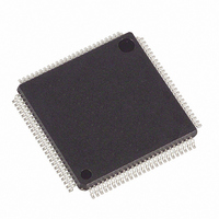
MAXQ2010-RFX+ Maxim Integrated Products, MAXQ2010-RFX+ Datasheet - Page 10

MAXQ2010-RFX+
Manufacturer Part Number
MAXQ2010-RFX+
Description
IC MCU 16BIT 64KB FLASH 100-LQFP
Manufacturer
Maxim Integrated Products
Series
MAXQ™r
Datasheet
1.MAXQ2010-RFX.pdf
(34 pages)
Specifications of MAXQ2010-RFX+
Core Processor
RISC
Core Size
16-Bit
Speed
10MHz
Connectivity
I²C, SPI, UART/USART
Peripherals
Brown-out Detect/Reset, LCD, POR, PWM, WDT
Number Of I /o
55
Program Memory Size
64KB (64K x 8)
Program Memory Type
FLASH
Ram Size
2K x 8
Voltage - Supply (vcc/vdd)
2.7 V ~ 3.6 V
Data Converters
A/D 8x12b
Oscillator Type
Internal
Operating Temperature
-40°C ~ 85°C
Package / Case
100-LQFP
Processor Series
MAXQ2010
Core
RISC
Data Bus Width
16 bit
Data Ram Size
2 KB
Interface Type
I2C, SPI, USART
Maximum Clock Frequency
10 MHz
Number Of Timers
3
Operating Supply Voltage
2.7 V to 3.6 V
Maximum Operating Temperature
+ 85 C
Mounting Style
SMD/SMT
Minimum Operating Temperature
- 40 C
Controller Family/series
MAXQ
No. Of I/o's
43
Ram Memory Size
2048Byte
Cpu Speed
10MHz
No. Of Timers
3
Embedded Interface Type
I2C, SPI, USART
Rohs Compliant
Yes
Number Of Programmable I/os
55
Development Tools By Supplier
MAXQ2010-KIT
Package
100LQFP
Family Name
MAXQ
Maximum Speed
10 MHz
On-chip Adc
8-chx12-bit
Lead Free Status / RoHS Status
Lead free / RoHS Compliant
Eeprom Size
-
Lead Free Status / Rohs Status
Lead free / RoHS Compliant
16-Bit Mixed-Signal Microcontroller
with LCD Interface
I
(V
Figure 3. Series Resistors (R
Note 19: Devices that use nonstandard supply voltages that do not conform to the intended I
Note 20: C
Note 21: The maximum fall time of 300ns for the SDA and SCL bus lines shown in the I
10
2
Input Low Voltage (Note 19)
Input High Voltage (Note 19)
Input Hysteresis (Schmitt)
Output Logic-Low (Open
Drain or Open Collector)
Output Fall Time from
V
Capacitance from 10pF to
400pF (Notes 20, 21)
Pulse Width of Spike
Filtering That Must Be
Suppressed by Input Filter
Input Current on I/O
I/O Capacitance
DVDD
IH_MIN
C ELECTRICAL CHARACTERISTICS
______________________________________________________________________________________
= V
PARAMETER
to V
input levels to the voltage to which the pullup resistors R
the specified maximum t
between the SDA/SCL pins and the SDA/SCL bus lines as shown in the I
table without exceeding the maximum specified fall time. See Figure 3.
AVDD
B
IL_MAX
—Capacitance of one bus line in pF.
= 2.7V to 3.6V, T
with Bus
S
) for Protecting Against High-Voltage Spikes
SYMBOL
V
V
C
V
t
t
V
IHYS_I2C
I
OF_I2C
SP_I2C
A
OL_I2C
IN_I2C
IH_I2C
IO_I2C
IL_I2C
OF_I2C
= -40°C to +85°C.)
MAXQ2010
of 250ns for the output stages. This allows series protection resistors (R
V
V
current
Input voltage from 0.1 x
V
DVDD
DVDD
DVDD
P6.7
P6.6
TEST CONDITIONS
SDA
SCL
> 2V
> 2V, 3mA sink
to 0.9 x V
DEVICE
DVDD
I
R
2
S
C
R
S
P
are connected. See Figure 3.
0.7 x V
STANDARD MODE
MIN
-0.5
-10
DEVICE
V
0
DVDD
I
R
2
DVDD
S
C
R
S
2
0.3 x V
C Bus Controller Timing (Acting as I
MAX
2
+10
250
0.4
10
C Bus Controller Timing table is longer than
DVDD
R
P
2
C bus system levels must relate their
R
0.05 x V
0.7 x V
20 + 0.1C
P
MIN
-0.5
-10
0
0
FAST MODE
DVDD
DVDD
B
V
0.3 x V
DVDD
S
) to be connected
MAX
+10
250
0.4
50
10
+ 0.5V
DVDD
2
C Slave)
UNITS
μA
pF
ns
ns
V
V
V
V


