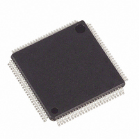
MAXQ2010-RFX+ Maxim Integrated Products, MAXQ2010-RFX+ Datasheet - Page 21

MAXQ2010-RFX+
Manufacturer Part Number
MAXQ2010-RFX+
Description
IC MCU 16BIT 64KB FLASH 100-LQFP
Manufacturer
Maxim Integrated Products
Series
MAXQ™r
Datasheet
1.MAXQ2010-RFX.pdf
(34 pages)
Specifications of MAXQ2010-RFX+
Core Processor
RISC
Core Size
16-Bit
Speed
10MHz
Connectivity
I²C, SPI, UART/USART
Peripherals
Brown-out Detect/Reset, LCD, POR, PWM, WDT
Number Of I /o
55
Program Memory Size
64KB (64K x 8)
Program Memory Type
FLASH
Ram Size
2K x 8
Voltage - Supply (vcc/vdd)
2.7 V ~ 3.6 V
Data Converters
A/D 8x12b
Oscillator Type
Internal
Operating Temperature
-40°C ~ 85°C
Package / Case
100-LQFP
Processor Series
MAXQ2010
Core
RISC
Data Bus Width
16 bit
Data Ram Size
2 KB
Interface Type
I2C, SPI, USART
Maximum Clock Frequency
10 MHz
Number Of Timers
3
Operating Supply Voltage
2.7 V to 3.6 V
Maximum Operating Temperature
+ 85 C
Mounting Style
SMD/SMT
Minimum Operating Temperature
- 40 C
Controller Family/series
MAXQ
No. Of I/o's
43
Ram Memory Size
2048Byte
Cpu Speed
10MHz
No. Of Timers
3
Embedded Interface Type
I2C, SPI, USART
Rohs Compliant
Yes
Number Of Programmable I/os
55
Development Tools By Supplier
MAXQ2010-KIT
Package
100LQFP
Family Name
MAXQ
Maximum Speed
10 MHz
On-chip Adc
8-chx12-bit
Lead Free Status / RoHS Status
Lead free / RoHS Compliant
Eeprom Size
-
Lead Free Status / Rohs Status
Lead free / RoHS Compliant
The following sections are an introduction to the prima-
ry features of the microcontroller. More detailed
descriptions of the device features can be found in the
errata sheets and user’s guides described later in the
Additional Documentation section.
The MAXQ2010 is a low-cost, high-performance,
CMOS, fully static, 16-bit RISC microcontroller with
flash memory and an integrated LCD controller. The
MAXQ2010 supports up to a 160-segment LCD and
supports 8 channels of high-performance measurement
using a 12-bit successive approximation register (SAR)
ADC with internal reference. The MAXQ2010 is struc-
tured on a highly advanced, accumulator-based, 16-bit
RISC architecture. Fetch and execution operations are
completed in one cycle without pipelining because the
instruction contains both the op code and data. The
result is a streamlined microcontroller performing at up
to one million instructions-per-second (MIPS) for each
MHz of the system operating frequency.
A 16-level hardware stack, enabling fast subroutine
calling and task switching, supports the highly efficient
core. Data can be quickly and efficiently manipulated
with three internal data pointers. Multiple data pointers
allow more than one function to access data memory
without having to save and restore data pointers each
time. The data pointers can automatically increment or
decrement following an operation, eliminating the need
for software intervention. As a result, application speed
is greatly increased.
The instruction set is composed of fixed-length, 16-bit
instructions that operate on registers and memory loca-
tions. The instruction set is highly orthogonal, allowing
arithmetic and logical operations to use any register
along with the accumulator. Special-function registers
control the peripherals and are subdivided into register
modules. The family architecture is modular so that new
devices and modules can reuse code developed for
existing products.
The architecture is transport-triggered, which means
that writes or reads from certain register locations can
also cause side effects to occur. These side effects
form the basis for the higher level op codes defined by
the assembler, such as ADDC, OR, JUMP, etc. The op
codes are actually implemented as MOVE instructions
between certain register locations, while the assembler
handles the encoding, which need not be a concern to
the programmer.
MAXQ Core Architecture
______________________________________________________________________________________
Detailed Description
16-Bit Mixed-Signal Microcontroller
Instruction Set
The 16-bit instruction word is designed for efficient exe-
cution. Bit 15 indicates the format for the source field of
the instruction. Bits 0 to 7 of the instruction represent
the source for the transfer. Depending on the value of
the format field, this can either be an immediate value
or a source register. If this field represents a register,
the lower four bits contain the module specifier and the
upper four bits contain the register index in that mod-
ule. Bits 8 to 14 represent the destination for the trans-
fer. This value always represents a destination register,
with the lower four bits containing the module specifier
and the upper three bits containing the register
subindex within that module. Any time that it is neces-
sary to directly select one of the upper 24 registers as a
destination, the prefix register (PFX) is needed to sup-
ply the extra destination bits. This prefix register write is
inserted automatically by the assembler and requires
only one additional execution cycle.
The device incorporates several memory areas, includ-
ing:
• 4KB utility ROM
• 64KB of flash memory for program storage
• 2KB of SRAM for storage of temporary variables
• 16-level stack memory for storage of program return
The incorporation of flash memory allows the devices to
be reprogrammed multiple times, allowing modifica-
tions to user applications post production. Additionally,
the flash can be used to store application information
including configuration data and log files.
The default memory organization is organized as a
Harvard architecture, with separate address spaces for
program and data memory. Pseudo-Von Neumann
memory organization is supported through the utility
ROM for applications that require dynamic program
modification and execution from RAM. The pseudo-Von
Neumann memory organization places the code, data,
and utility ROM memories into a single contiguous
memory map. See Figure 5 for the memory map.
A 16-bit-wide hardware stack provides storage for pro-
gram return addresses and can also be used as gener-
al-purpose data storage. The stack is used
automatically by the processor when the CALL, RET,
and RETI instructions are executed and when an inter-
rupt is serviced. An application can also store values in
the stack explicitly by using the PUSH, POP, and POPI
instructions.
addresses and general-purpose use
with LCD Interface
Memory Organization
Stack Memory
21


