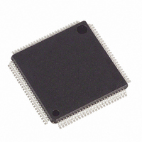
MAXQ2010-RFX+ Maxim Integrated Products, MAXQ2010-RFX+ Datasheet - Page 8

MAXQ2010-RFX+
Manufacturer Part Number
MAXQ2010-RFX+
Description
IC MCU 16BIT 64KB FLASH 100-LQFP
Manufacturer
Maxim Integrated Products
Series
MAXQ™r
Datasheet
1.MAXQ2010-RFX.pdf
(34 pages)
Specifications of MAXQ2010-RFX+
Core Processor
RISC
Core Size
16-Bit
Speed
10MHz
Connectivity
I²C, SPI, UART/USART
Peripherals
Brown-out Detect/Reset, LCD, POR, PWM, WDT
Number Of I /o
55
Program Memory Size
64KB (64K x 8)
Program Memory Type
FLASH
Ram Size
2K x 8
Voltage - Supply (vcc/vdd)
2.7 V ~ 3.6 V
Data Converters
A/D 8x12b
Oscillator Type
Internal
Operating Temperature
-40°C ~ 85°C
Package / Case
100-LQFP
Processor Series
MAXQ2010
Core
RISC
Data Bus Width
16 bit
Data Ram Size
2 KB
Interface Type
I2C, SPI, USART
Maximum Clock Frequency
10 MHz
Number Of Timers
3
Operating Supply Voltage
2.7 V to 3.6 V
Maximum Operating Temperature
+ 85 C
Mounting Style
SMD/SMT
Minimum Operating Temperature
- 40 C
Controller Family/series
MAXQ
No. Of I/o's
43
Ram Memory Size
2048Byte
Cpu Speed
10MHz
No. Of Timers
3
Embedded Interface Type
I2C, SPI, USART
Rohs Compliant
Yes
Number Of Programmable I/os
55
Development Tools By Supplier
MAXQ2010-KIT
Package
100LQFP
Family Name
MAXQ
Maximum Speed
10 MHz
On-chip Adc
8-chx12-bit
Lead Free Status / RoHS Status
Lead free / RoHS Compliant
Eeprom Size
-
Lead Free Status / Rohs Status
Lead free / RoHS Compliant
16-Bit Mixed-Signal Microcontroller
with LCD Interface
RECOMMENDED DC OPERATING CONDITIONS (continued)
(V
Note 12: Programming time does not include overhead associated with the utility ROM interface.
Note 13: V
Note 14: The operational input voltage range for each individual input of a differentially configured pair is from GND to AVDD. The
Note 15: The typical value is applied when a conversion is requested with ADPMO = 0. Under these conditions, the minimum delay
Note 16: Switching ADC reference from either internal or external reference to AVDD. Sample accuracy is not guaranteed prior to
Note 17: Total on-board decoupling capacitance on the AVDD pin < 100nF. The output impedance of the regulator driving the
Note 18: This parameter is guaranteed by design and is not production tested.
8
SPI (See Figures 1 and 2)
SPI Master Operating Frequency
SPI Slave Operating Frequency
SCLK Output Pulse-Width
High/Low
SCLK Input Pulse-Width
High/Low
MOSI Output Hold Time After
SCLK Sample Edge
MOSI Output Valid to Sample
Edge
MISO Input Valid to SCLK
Sample Edge Rise/Fall Setup
MISO Input to SCLK Sample
Edge Rise/Fall Hold
SCLK Inactive to MOSI Inactive
SSEL Active to First Shift Edge
MOSI Input to SCLK Sample
Edge Rise/Fall Setup
MOSI Input from SCLK Sample
Edge Transition Hold
MISO Output Valid After SCLK
Shift Edge Transition
SSEL Inactive
SCLK Inactive to SSEL Rising
MISO Output Disabled After
SSEL Edge Rise
DVDD
_______________________________________________________________________________________
= V
PARAMETER
operational input voltage difference is from -V
is met. If ADPMO = 1, the user is responsible for ensuring the 4µs delay time is met.
ADC reference settlement.
AVDD pin < 10Ω.
AVDD
REF
= V
= 2.7V to 3.6V, T
AVDD
.
A
= -40°C to +85°C.) (Note 1)
t
t
SYMBOL
MCH
SCH
1/t
1/t
t
t
t
t
t
t
t
t
t
MOH
MOV
t
t
MLH
SOV
t
MIS
MIH
SSE
SSH
SLH
SIS
SIH
MCK
SD
SCK
, t
, t
MCL
SCL
C
L
= 50pF
REF
/2 to +V
CONDITIONS
REF
/2.
(t
(t
(t
(t
MCK
MCK
MCK
MCK
t
t
t
4t
CK
CK
CK
- 25
- 25
- 25
- 25
MIN
25
20
25
25
25
0
CK
+
+
+
/2)
/2)
/2)
/2)
t
SCK
TYP
/2
3t
2t
f
f
MAX
CK
CK
CK
CK
25
50
/2
/8
+
+
UNITS
MHz
MHz
ns
ns
ns
ns
ns
ns
ns
ns
ns
ns
ns
ns
ns
ns


