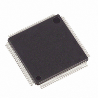
MAXQ2010-RFX+ Maxim Integrated Products, MAXQ2010-RFX+ Datasheet - Page 4

MAXQ2010-RFX+
Manufacturer Part Number
MAXQ2010-RFX+
Description
IC MCU 16BIT 64KB FLASH 100-LQFP
Manufacturer
Maxim Integrated Products
Series
MAXQ™r
Datasheet
1.MAXQ2010-RFX.pdf
(34 pages)
Specifications of MAXQ2010-RFX+
Core Processor
RISC
Core Size
16-Bit
Speed
10MHz
Connectivity
I²C, SPI, UART/USART
Peripherals
Brown-out Detect/Reset, LCD, POR, PWM, WDT
Number Of I /o
55
Program Memory Size
64KB (64K x 8)
Program Memory Type
FLASH
Ram Size
2K x 8
Voltage - Supply (vcc/vdd)
2.7 V ~ 3.6 V
Data Converters
A/D 8x12b
Oscillator Type
Internal
Operating Temperature
-40°C ~ 85°C
Package / Case
100-LQFP
Processor Series
MAXQ2010
Core
RISC
Data Bus Width
16 bit
Data Ram Size
2 KB
Interface Type
I2C, SPI, USART
Maximum Clock Frequency
10 MHz
Number Of Timers
3
Operating Supply Voltage
2.7 V to 3.6 V
Maximum Operating Temperature
+ 85 C
Mounting Style
SMD/SMT
Minimum Operating Temperature
- 40 C
Controller Family/series
MAXQ
No. Of I/o's
43
Ram Memory Size
2048Byte
Cpu Speed
10MHz
No. Of Timers
3
Embedded Interface Type
I2C, SPI, USART
Rohs Compliant
Yes
Number Of Programmable I/os
55
Development Tools By Supplier
MAXQ2010-KIT
Package
100LQFP
Family Name
MAXQ
Maximum Speed
10 MHz
On-chip Adc
8-chx12-bit
Lead Free Status / RoHS Status
Lead free / RoHS Compliant
Eeprom Size
-
Lead Free Status / Rohs Status
Lead free / RoHS Compliant
16-Bit Mixed-Signal Microcontroller
with LCD Interface
ABSOLUTE MAXIMUM RATINGS
Voltage Range on All Pins (including AVDD,
Voltage Range on Any Pin Relative to
Operating Temperature Range ...........................-40°C to +85°C
RECOMMENDED DC OPERATING CONDITIONS
(V
Stresses beyond those listed under “Absolute Maximum Ratings” may cause permanent damage to the device. These are stress ratings only, and functional
operation of the device at these or any other conditions beyond those indicated in the operational sections of the specifications is not implied. Exposure to
absolute maximum rating conditions for extended periods may affect device reliability.
4
Input Low Voltage on HFXIN and
32KIN
Digital Supply Voltage
Digital Supply Voltage Output
Analog Supply Voltage
Ground
Digital Power-Fail Reset Voltage
Active Current, FLL Disabled
(Note 3)
Active Current, FLL Enabled
(Note 5)
Stop-Mode Current
(Note 6)
Stop-Mode Resume Time
(Note 4)
Input Low Voltage on All Other
Pins
DVDD) Relative to Ground .................................-0.5V to +3.6V
Ground Except AVDD, DVDD .............-0.5V to (V
DVDD
_______________________________________________________________________________________
= V
PARAMETER
AVDD
= 2.7V to 3.6V, T
A
= -40°C to +85°C.) (Note 1)
SYMBOL
V
I
I
I
I
I
I
I
(Note 7)
(Note 8)
(Note 9)
I
I
I
t
t
t
DD_HFX1
DD_HFX2
DD1_FLL
DD2_FLL
DD3_FLL
DD4_FLL
DD5_FLL
REGOUT
V
V
STOP_1
STOP_2
STOP_3
STOP_1
STOP_2
STOP_3
GND
V
DVDD
AVDD
V
V
RST
IL1
IL2
DVDD
(Note 2)
V
AGND = DGND
Monitors V
f
FREQMD = 0
f
FREQMD = 0 (Note 4)
Divide-by-1 mode, FREQMD = 0
Divide-by-2 mode, FREQMD = 0 (Note 4)
Divide-by-4 mode, FREQMD = 1 (Note 4)
Divide-by-8 mode, FREQMD = 1 (Note 4)
PMM mode, FREQMD = 1 (Note 4)
T
T
T
T
T
T
Internal regulator on
Internal regulator off, brownout or SVM on,
SVMSTOP = 1
Internal regulator, brownout, and SVM off
CK
CK
A
A
A
A
A
A
AVDD
= +25°C
= +85°C
= +25°C
= +85°C
= +25°C
= +85°C
= 10MHz, V
= 10MHz, V
+ 0.5V)
= V
DVDD
DVDD
CONDITIONS
DVDD
DVDD
Continuous Output Current
Storage Temperature Range .............................-65°C to +150°C
Soldering Temperature...........................Refer to the IPC/JEDEC
Any Single I/O Pin ............................................................20mA
All I/O Pins Combined....................................................100mA
= V
= V
AVDD
AVDD
= 2.7V,
= 3.6V,
DGND
DGND
2.55
MIN
2.7
2.7
0
4t
TYP
3.15
2.25
0.37
0.68
0.94
195
225
1.8
2.6
3.1
3.2
2.9
1.4
0.5
1.3
CLCL
30
30
J-STD-020 Specification.
0.20 x
V
0.30 x
V
MAX
2.65
3.75
DVDD
DVDD
295
335
160
320
3.6
3.6
4.0
3.6
0.7
6.5
6.5
0
4
3
2
4
5
UNITS
mA
mA
μA
μs
V
V
V
V
V
V
V


