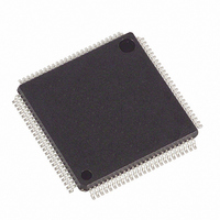
MAXQ2010-RFX+ Maxim Integrated Products, MAXQ2010-RFX+ Datasheet - Page 11

MAXQ2010-RFX+
Manufacturer Part Number
MAXQ2010-RFX+
Description
IC MCU 16BIT 64KB FLASH 100-LQFP
Manufacturer
Maxim Integrated Products
Series
MAXQ™r
Datasheet
1.MAXQ2010-RFX.pdf
(34 pages)
Specifications of MAXQ2010-RFX+
Core Processor
RISC
Core Size
16-Bit
Speed
10MHz
Connectivity
I²C, SPI, UART/USART
Peripherals
Brown-out Detect/Reset, LCD, POR, PWM, WDT
Number Of I /o
55
Program Memory Size
64KB (64K x 8)
Program Memory Type
FLASH
Ram Size
2K x 8
Voltage - Supply (vcc/vdd)
2.7 V ~ 3.6 V
Data Converters
A/D 8x12b
Oscillator Type
Internal
Operating Temperature
-40°C ~ 85°C
Package / Case
100-LQFP
Processor Series
MAXQ2010
Core
RISC
Data Bus Width
16 bit
Data Ram Size
2 KB
Interface Type
I2C, SPI, USART
Maximum Clock Frequency
10 MHz
Number Of Timers
3
Operating Supply Voltage
2.7 V to 3.6 V
Maximum Operating Temperature
+ 85 C
Mounting Style
SMD/SMT
Minimum Operating Temperature
- 40 C
Controller Family/series
MAXQ
No. Of I/o's
43
Ram Memory Size
2048Byte
Cpu Speed
10MHz
No. Of Timers
3
Embedded Interface Type
I2C, SPI, USART
Rohs Compliant
Yes
Number Of Programmable I/os
55
Development Tools By Supplier
MAXQ2010-KIT
Package
100LQFP
Family Name
MAXQ
Maximum Speed
10 MHz
On-chip Adc
8-chx12-bit
Lead Free Status / RoHS Status
Lead free / RoHS Compliant
Eeprom Size
-
Lead Free Status / Rohs Status
Lead free / RoHS Compliant
I
(V
Note 22: All values referenced to V
Note 23: A device must internally provide a hold time of at least 300ns for the SDA signal (referred to as the V
Note 24: The maximum t
Note 25: A fast-mode I
Note 26: C
2
Operating Frequency
Hold Time After (Repeated)
START
Clock Low Period
Clock High Period
Setup Time for Repeated START
Hold Time for Data
Setup Time for Data
SDA/SCL Fall Time
SDA/SCL Rise Time
Setup Time for STOP
Bus-Free Time Between STOP
and START
Capacitive Load for Each Bus
Line
Noise Margin at the Low Level
for Each Connected Device
(Including Hysteresis)
Noise Margin at the High Level
for Each Connected Device
(Including Hysteresis)
DVDD
C BUS CONTROLLER TIMING
= V
PARAMETER
signal) to bridge the undefined region of the falling edge of SCL.
be met. This is automatically the case if the device does not stretch the low period of the SCL signal. If such a device does
stretch the low period of the SCL signal, it must output the next data bit to the SDA line t
= 1250ns (according to the standard-mode I
AVDD
B
—Total capacitance of one bus line in pF.
= 2.7V to 3.6V, T
______________________________________________________________________________________
2
C bus device can be used in a standard-mode I
HD:DAT
need only be met if the device does not stretch the low period (t
A
16-Bit Mixed-Signal Microcontroller
= -40°C to +85°C.) (Note 22) (Figure 4)
IH_I2C(MIN)
SYMBOL
t
t
HIGH_I2C
t
V
t
LOW_I2C
t
t
t
V
HD:STA
SU:STA
HD:DAT
SU:DAT
SU:STO
t
t
NH_I2C
NL_I2C
R_I2C
F_I2C
t
f
BUF
C
I2C
B
and V
0.1 x V
0.2 x V
IL_I2C(MAX)
(Note 23)
2
MIN
250
C specification) before the SCL line is released.
4.0
4.7
4.0
4.7
4.0
4.7
STANDARD MODE
0
0
DVDD
DVDD
.
(Note 24)
2
MAX
1000
C bus system, but the requirement t
3.45
100
300
400
with LCD Interface
0.1 x V
0.2 x V
20 + 0.1C
20 + 0.1C
(Note 23)
(Note 25)
(Note 26)
(Note 26)
MIN
100
0.6
1.3
0.6
0.6
0.6
1.3
0
0
DVDD
DVDD
LOW_I2C
FAST MODE
R_I2C(MAX)
B
B
) of the SCL signal.
(Note 24)
+ t
SU:DAT
IH_I2C(MIN)
MAX
400
300
300
400
SU:DAT
0.9
≥ 250ns must
= 1000 + 250
of the SCL
UNITS
kHz
μs
μs
μs
μs
μs
ns
ns
ns
μs
μs
pF
V
V
11


