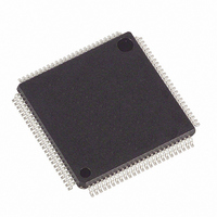
MAXQ2010-RFX+ Maxim Integrated Products, MAXQ2010-RFX+ Datasheet - Page 19

MAXQ2010-RFX+
Manufacturer Part Number
MAXQ2010-RFX+
Description
IC MCU 16BIT 64KB FLASH 100-LQFP
Manufacturer
Maxim Integrated Products
Series
MAXQ™r
Datasheet
1.MAXQ2010-RFX.pdf
(34 pages)
Specifications of MAXQ2010-RFX+
Core Processor
RISC
Core Size
16-Bit
Speed
10MHz
Connectivity
I²C, SPI, UART/USART
Peripherals
Brown-out Detect/Reset, LCD, POR, PWM, WDT
Number Of I /o
55
Program Memory Size
64KB (64K x 8)
Program Memory Type
FLASH
Ram Size
2K x 8
Voltage - Supply (vcc/vdd)
2.7 V ~ 3.6 V
Data Converters
A/D 8x12b
Oscillator Type
Internal
Operating Temperature
-40°C ~ 85°C
Package / Case
100-LQFP
Processor Series
MAXQ2010
Core
RISC
Data Bus Width
16 bit
Data Ram Size
2 KB
Interface Type
I2C, SPI, USART
Maximum Clock Frequency
10 MHz
Number Of Timers
3
Operating Supply Voltage
2.7 V to 3.6 V
Maximum Operating Temperature
+ 85 C
Mounting Style
SMD/SMT
Minimum Operating Temperature
- 40 C
Controller Family/series
MAXQ
No. Of I/o's
43
Ram Memory Size
2048Byte
Cpu Speed
10MHz
No. Of Timers
3
Embedded Interface Type
I2C, SPI, USART
Rohs Compliant
Yes
Number Of Programmable I/os
55
Development Tools By Supplier
MAXQ2010-KIT
Package
100LQFP
Family Name
MAXQ
Maximum Speed
10 MHz
On-chip Adc
8-chx12-bit
Lead Free Status / RoHS Status
Lead free / RoHS Compliant
Eeprom Size
-
Lead Free Status / Rohs Status
Lead free / RoHS Compliant
10, 9, 8
PIN
68
67
61
60
59
58
57
32
31
7
COM1; SEG40,
SEG41, SEG42
COM3, COM2,
P5.2/INT10/
P5.3/INT11/
P5.4/INT12/
P5.5/INT13/
P5.6/INT14/
P6.0/INT15/
P6.1/INT16/
P5.0/INT8/
TB0B/RX0
P5.1/INT9/
TB0A/TX0
______________________________________________________________________________________
NAME
COM0
MOSI
SCLK
MISO
SSEL
SQW
TCK
TDI
LCD Segment-Driver Output; LCD Common Drive Output. These pins function as LCD
segment or common drive outputs. Configuring a pin as a common drive output disables the
segment function for that pin.
LCD Common Drive 0, Output. This pin functions as a LCD common-drive output.
Digital I/O, Type D Port 5.0; Timer B0 Pin B; Serial Port 0 Receive; External Edge-Selectable
Interrupt 8. This pin defaults to an input with a weak pullup after reset and functions as
general-purpose I/O. The port pad contains a Schmitt voltage input and can be configured as
an external interrupt. Enabling a special function disables the pin as digital I/O.
Digital I/O, Type D Port 5.1; Timer B0 Pin A; Serial Port 0 Transmit; External Edge-
Selectable Interrupt 9. This pin defaults to an input with a weak pullup after reset and
functions as general-purpose I/O. The port pad contains a Schmitt voltage input and can be
configured as an external interrupt. Enabling a special function disables the pin as general-
purpose I/O.
Digital I/O, Type-D Port 5.2; External Edge-Selectable Interrupt 10; RTC Square-Wave Output.
This pin defaults to an input with a weak pullup after reset and functions as general-purpose
I/O. The port pad contains a Schmitt voltage input and can be configured as an external
interrupt. Enabling a special function disables the pin as general-purpose I/O.
Digital I/O, Type D Port 5.3; External Edge-Selectable Interrupt 11; Active-Low SPI Slave-
Select Input. This pin defaults to an input with a weak pullup after reset and functions as
general-purpose I/O. The port pad contains a Schmitt voltage input and can be configured as
an external interrupt. Enabling a special function disables the pin as general-purpose I/O.
Digital I/O, Type D Port 5.4; External Edge-Selectable Interrupt 12; SPI Master Out-Slave In.
This pin defaults to an input with a weak pullup after reset and functions as general-purpose
I/O. The port pad contains a Schmitt voltage input and can be configured as an external
interrupt. Enabling a special function disables the pin as general-purpose I/O.
Digital I/O, Type D Port 5.5; External Edge-Selectable Interrupt 13; SPI Clock Output. This pin
defaults as an input with a weak pullup after a reset and functions as general-purpose I/O. The
port pad contains a Schmitt input circuitry and can be configured as an external interrupt.
Enabling a special function disables the pin as general-purpose I/O.
Digital I/O, Type D Port 5.6; External Edge-Selectable Interrupt 14; SPI Master In-Slave Out.
This pin defaults to an input with a weak pullup after reset and functions as general-purpose
I/O. The port pad contains a Schmitt voltage input and can be configured as an external
interrupt. Enabling a special function disables the pin as general-purpose I/O.
Digital I/O, Type D Port 6.0; External Edge-Selectable Interrupt 15; JTAG Test Clock Input.
This pin defaults to an input with a weak pullup after reset and functions as general-purpose
I/O. The port pad contains a Schmitt voltage input and can be configured as an external
interrupt. Enabling a special function disables the pin as general-purpose I/O.
Digital I/O, Type D Port 6.1; External Edge-Selectable Interrupt 16; JTAG Test Data Input.
This pin defaults to an input with a weak pullup after reset and functions as general-purpose
I/O. The port pad contains a Schmitt voltage input and can be configured as an external
interrupt. Enabling a special function disables the pin as general-purpose I/O.
16-Bit Mixed-Signal Microcontroller
PIN
10
9
8
COM3
COM2
COM1
FUNCTION
SPECIAL/ALTERNATE FUNCTION
with LCD Interface
Pin Description (continued)
SEG40
SEG41
SEG42
19


