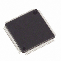
MAXQ2010-RFX+ Maxim Integrated Products, MAXQ2010-RFX+ Datasheet - Page 28

MAXQ2010-RFX+
Manufacturer Part Number
MAXQ2010-RFX+
Description
IC MCU 16BIT 64KB FLASH 100-LQFP
Manufacturer
Maxim Integrated Products
Series
MAXQ™r
Datasheet
1.MAXQ2010-RFX.pdf
(34 pages)
Specifications of MAXQ2010-RFX+
Core Processor
RISC
Core Size
16-Bit
Speed
10MHz
Connectivity
I²C, SPI, UART/USART
Peripherals
Brown-out Detect/Reset, LCD, POR, PWM, WDT
Number Of I /o
55
Program Memory Size
64KB (64K x 8)
Program Memory Type
FLASH
Ram Size
2K x 8
Voltage - Supply (vcc/vdd)
2.7 V ~ 3.6 V
Data Converters
A/D 8x12b
Oscillator Type
Internal
Operating Temperature
-40°C ~ 85°C
Package / Case
100-LQFP
Processor Series
MAXQ2010
Core
RISC
Data Bus Width
16 bit
Data Ram Size
2 KB
Interface Type
I2C, SPI, USART
Maximum Clock Frequency
10 MHz
Number Of Timers
3
Operating Supply Voltage
2.7 V to 3.6 V
Maximum Operating Temperature
+ 85 C
Mounting Style
SMD/SMT
Minimum Operating Temperature
- 40 C
Controller Family/series
MAXQ
No. Of I/o's
43
Ram Memory Size
2048Byte
Cpu Speed
10MHz
No. Of Timers
3
Embedded Interface Type
I2C, SPI, USART
Rohs Compliant
Yes
Number Of Programmable I/os
55
Development Tools By Supplier
MAXQ2010-KIT
Package
100LQFP
Family Name
MAXQ
Maximum Speed
10 MHz
On-chip Adc
8-chx12-bit
Lead Free Status / RoHS Status
Lead free / RoHS Compliant
Eeprom Size
-
Lead Free Status / Rohs Status
Lead free / RoHS Compliant
16-Bit Mixed-Signal Microcontroller
with LCD Interface
(ADPMO = 0), the ADC waits for 20 ADCCLK before
starting the first conversion. This allows the ADC time to
set up.
If ADPMO = 1, an ADC conversion is initiated as soon
as ADCONV is set to 1. ADC operation is aborted upon
entry into PMM or stop mode.
The ADCONV bit is set at the beginning of the conver-
sion process and remains set until the conversion
process is finished. In single-sequence mode, this bit
remains set until the ADC has finished conversion on
the last channel in the sequence. In continuous mode,
the ADCONV bit remains set until the continuous mode
is stopped. Writing a 0 to the ADCONV bit stops ADC
operation at the completion of the current ADC conver-
sion. The new data is written to the data buffer.
An A/D conversion takes 16 ADCCLK cycles to com-
plete. Three of the 16 ADCCLK cycles are used for
sample acquisition. The ADCCLK is derived from the
system clock with divide ratio defined by the ADC clock
divider bits (ADCCLK). Therefore, with 16 ADCCLK to
acquire one data, the fastest ADC rate = sysclk/16
(ADCCLK = 0h, ADACQEN = 0h). With a 10MHz sys-
tem clock, this is theoretically equivalent to 10MHz/16
value Msps. Note, however, that the ADC conversion is
limited to 300ksps.
If the ADC data-available interrupt is enabled (ADDAIE
= 1), an interrupt is generated to the CPU when ADDAI
= 1. Once set, the ADDAI flag can be cleared by soft-
ware writing a 0 or at the start of a conversion process
when ADCONV is set to 1. The data-available interrupt
flag (ADDAI) can optionally be set by using the ADC
data-available interrupt interval bits (ADDAINV). The
Figure 7. ADC Block Diagram
28
______________________________________________________________________________________
REFERENCE
REFERENCE
EXTERNAL
INTERNAL
AVDD
ADC REFERENCE
AVDD
AVSS
ADC CONTROL
12-BIT
SAR
ADDAI can be set in 1, 2, 3, 4, 5, 6, 7, 8, 12, or 16 sam-
ples intervals. For a sequence that uses only one con-
figuration register, setting ADDAINV = 00 generates an
interrupt with the same interval as ADDAINV = 01, both
of which set the ADDAI at every ADC sample. When the
ADDAI is set, the last memory location written by ADC
will also be written to ADDADDR.
The MAXQ2010 microcontroller incorporates an LCD
controller that interfaces to common low-voltage dis-
plays. By incorporating the LCD controller into the
microcontroller, the design requires only an LCD glass
rather than a considerably more expensive LCD mod-
ule. Every character in an LCD glass is composed of
one or more segments, each of which is activated by
selecting the appropriate segment and common signal.
The microcontroller can multiplex combinations of up to
43 segment outputs (SEG0 to SEG42) and four com-
mon signal outputs (COM0 to COM3). Unused segment
outputs can be used as general-purpose port pins.
The segments are easily addressed by writing to dedi-
cated display memory. Once the LCD controller set-
tings and display memory have been initialized, the
21-byte display memory is periodically scanned, and
the segment and common signals are generated auto-
matically at the selected display frequency. No addi-
tional processor overhead is required while the LCD
controller is running. Unused display memory can be
used for general-purpose storage.
The design is further simplified and cost reduced by
the inclusion of software-adjustable internal voltage-
MULTIPLEXER
TRACK/HOLD
INPUT
AND
ADC INTERRUPT
AN7
AN6
AN5
AN4
AN3
AN2
AN1
AN0
LCD Controller


