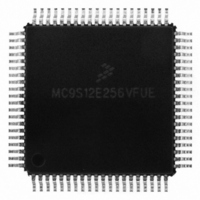
MC9S12E256VFUE Freescale Semiconductor, MC9S12E256VFUE Datasheet - Page 326

MC9S12E256VFUE
Manufacturer Part Number
MC9S12E256VFUE
Description
IC MCU 256K FLASH 25MHZ 80-QFP
Manufacturer
Freescale Semiconductor
Series
HCS12r
Datasheet
1.MC9S12E256CFUE.pdf
(602 pages)
Specifications of MC9S12E256VFUE
Core Processor
HCS12
Core Size
16-Bit
Speed
25MHz
Connectivity
EBI/EMI, I²C, SCI, SPI
Peripherals
POR, PWM, WDT
Number Of I /o
60
Program Memory Size
256KB (256K x 8)
Program Memory Type
FLASH
Ram Size
16K x 8
Voltage - Supply (vcc/vdd)
2.35 V ~ 2.75 V
Data Converters
A/D 16x10b; D/A 2x8b
Oscillator Type
Internal
Operating Temperature
-40°C ~ 105°C
Package / Case
80-QFP
Processor Series
S12E
Core
HCS12
Data Bus Width
16 bit
Data Ram Size
16 KB
Interface Type
I2C, SCI, SPI
Maximum Clock Frequency
50 MHz
Number Of Programmable I/os
60
Number Of Timers
12
Maximum Operating Temperature
+ 105 C
Mounting Style
SMD/SMT
3rd Party Development Tools
EWHCS12
Minimum Operating Temperature
- 40 C
On-chip Adc
10 bit, 16 Channel
On-chip Dac
8 bit, 2 Channel
Package
80PQFP
Family Name
HCS12
Maximum Speed
50 MHz
For Use With
M68EVB912E128 - BOARD EVAL FOR MC9S12E128/64
Lead Free Status / RoHS Status
Lead free / RoHS Compliant
Eeprom Size
-
Lead Free Status / Rohs Status
Details
Available stocks
Company
Part Number
Manufacturer
Quantity
Price
Company:
Part Number:
MC9S12E256VFUE
Manufacturer:
Freescale Semiconductor
Quantity:
10 000
- Current page: 326 of 602
- Download datasheet (4Mb)
Chapter 11 Pulse Width Modulator with Fault Protection (PMF15B6CV2)
11.3.2
The address of a register is the sum of a base address and an address offset. The base address is defined at
the chip level and the address offset is defined at the module level.
11.3.2.1
Read anytime.
See bit description for write conditions.
326
Module Base + 0x0000
EDGEC
EDGEB
Reset
Field
MTG
WP
7
6
5
4
W
R
Register Descriptions
Write Protect — This bit enables write protection to be used for all write-protectable registers. While clear, WP
allows write-protected registers to be written. When set, WP prevents any further writes to write-protected
registers. Once set, WP can be cleared only by reset.
0 Write-protectable registers may be written.
1 Write-protectable registers are write-protected.
Multiple Timebase Generators — This bit determines the number of timebase counters used. Once set, MTG
can be cleared only by reset.
If MTG is set, PWM generators B and C and registers $xx28–$xx37 are available. The three generators have
their own variable frequencies and are not synchronized.
If MTG is cleared, PMF registers from $xx28–$xx37 can not be written and read zeroes, and bits EDGEC and
EDGEB are ignored. Pair A, Pair B and Pair C PWMs are synchronized to PWM generator A and use registers
from $xx20–$xx27.
0 Single timebase generator.
1 Multiple timebase generators.
Edge-Aligned or Center-Aligned PWM for Pair C — This bit determines whether PWM4 and PWM5 channels
will use edge-aligned or center-aligned waveforms. This bit has no effect if MTG bit is cleared. This bit cannot be
modified after the WP bit is set.
0 PWM4 and PWM5 are center-aligned PWMs
1 PWM4 and PWM5 are edge-aligned PWMs
Edge-Aligned or Center-Aligned PWM for Pair B — This bit determines whether PWM2 and PWM3 channels
will use edge-aligned or center-aligned waveforms. This bit has no effect if MTG bit is cleared. This bit cannot be
modified after the WP bit is set.
0 PWM2 and PWM3 are center-aligned PWMs
1 PWM2 and PWM3 are edge-aligned PWMs
WP
PMF Configure 0 Register (PMFCFG0)
0
7
MTG
0
6
Figure 11-4. PMF Configure 0 Register (PMFCFG0)
Table 11-2. PMFCFG0 Field Descriptions
EDGEC
MC9S12E256 Data Sheet, Rev. 1.08
0
5
EDGEB
0
4
Description
EDGEA
3
0
INDEPC
0
2
INDEPB
Freescale Semiconductor
0
1
INDEPA
0
0
Related parts for MC9S12E256VFUE
Image
Part Number
Description
Manufacturer
Datasheet
Request
R
Part Number:
Description:
Manufacturer:
Freescale Semiconductor, Inc
Datasheet:
Part Number:
Description:
Manufacturer:
Freescale Semiconductor, Inc
Datasheet:
Part Number:
Description:
Manufacturer:
Freescale Semiconductor, Inc
Datasheet:
Part Number:
Description:
Manufacturer:
Freescale Semiconductor, Inc
Datasheet:
Part Number:
Description:
Manufacturer:
Freescale Semiconductor, Inc
Datasheet:
Part Number:
Description:
Manufacturer:
Freescale Semiconductor, Inc
Datasheet:
Part Number:
Description:
Manufacturer:
Freescale Semiconductor, Inc
Datasheet:
Part Number:
Description:
Manufacturer:
Freescale Semiconductor, Inc
Datasheet:
Part Number:
Description:
Manufacturer:
Freescale Semiconductor, Inc
Datasheet:
Part Number:
Description:
Manufacturer:
Freescale Semiconductor, Inc
Datasheet:
Part Number:
Description:
Manufacturer:
Freescale Semiconductor, Inc
Datasheet:
Part Number:
Description:
Manufacturer:
Freescale Semiconductor, Inc
Datasheet:
Part Number:
Description:
Manufacturer:
Freescale Semiconductor, Inc
Datasheet:
Part Number:
Description:
Manufacturer:
Freescale Semiconductor, Inc
Datasheet:
Part Number:
Description:
Manufacturer:
Freescale Semiconductor, Inc
Datasheet:


