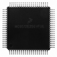
MC9S12E256VFUE Freescale Semiconductor, MC9S12E256VFUE Datasheet - Page 84

MC9S12E256VFUE
Manufacturer Part Number
MC9S12E256VFUE
Description
IC MCU 256K FLASH 25MHZ 80-QFP
Manufacturer
Freescale Semiconductor
Series
HCS12r
Datasheet
1.MC9S12E256CFUE.pdf
(602 pages)
Specifications of MC9S12E256VFUE
Core Processor
HCS12
Core Size
16-Bit
Speed
25MHz
Connectivity
EBI/EMI, I²C, SCI, SPI
Peripherals
POR, PWM, WDT
Number Of I /o
60
Program Memory Size
256KB (256K x 8)
Program Memory Type
FLASH
Ram Size
16K x 8
Voltage - Supply (vcc/vdd)
2.35 V ~ 2.75 V
Data Converters
A/D 16x10b; D/A 2x8b
Oscillator Type
Internal
Operating Temperature
-40°C ~ 105°C
Package / Case
80-QFP
Processor Series
S12E
Core
HCS12
Data Bus Width
16 bit
Data Ram Size
16 KB
Interface Type
I2C, SCI, SPI
Maximum Clock Frequency
50 MHz
Number Of Programmable I/os
60
Number Of Timers
12
Maximum Operating Temperature
+ 105 C
Mounting Style
SMD/SMT
3rd Party Development Tools
EWHCS12
Minimum Operating Temperature
- 40 C
On-chip Adc
10 bit, 16 Channel
On-chip Dac
8 bit, 2 Channel
Package
80PQFP
Family Name
HCS12
Maximum Speed
50 MHz
For Use With
M68EVB912E128 - BOARD EVAL FOR MC9S12E128/64
Lead Free Status / RoHS Status
Lead free / RoHS Compliant
Eeprom Size
-
Lead Free Status / Rohs Status
Details
Available stocks
Company
Part Number
Manufacturer
Quantity
Price
Company:
Part Number:
MC9S12E256VFUE
Manufacturer:
Freescale Semiconductor
Quantity:
10 000
- Current page: 84 of 602
- Download datasheet (4Mb)
Chapter 2 256 Kbyte Flash Module (FTS256K2V1)
2.2
The Flash module contains no signals that connect off-chip.
2.3
This subsection describes the memory map and registers for the Flash module.
2.3.1
The Flash memory map is shown in
addresses between 0x4000 and 0xFFFF which corresponds to three 16-Kbyte pages. The content of the
HCS12 core PPAGE register is used to map the logical middle page ranging from address 0x8000 to
0xBFFF to any physical 16 Kbyte page in the Flash memory. By placing 0x3E or 0x3F in the HCS12 Core
PPAGE register, the associated 16 Kbyte pages appear twice in the MCU memory map.
The FPROT register, described in
globally protect a Flash block. However, three separate memory regions, one growing upward from the
first address in the next-to-last page in the Flash block (called the lower region), one growing downward
from the last address in the last page in the Flash block (called the higher region), and the remaining
addresses in the Flash block, can be activated for protection. The Flash locations of these protectable
regions are shown in
boot loader code because it covers the vector space. The lower address region of any Flash block can be
used for EEPROM emulation in an MCU without an EEPROM module because it can remain unprotected
while the remaining addresses are protected from program or erase.
Security information that allows the MCU to restrict access to the Flash module is stored in the Flash
configuration field found in Flash block 0, described in
84
0xFF08 – 0xFF0B
0xFF00 – 0xFF07
Flash Address
Unpaged
0xFF0C
0xFF0D
0xFF0E
0xFF0F
External Signal Description
Memory Map and Register Definition
Module Memory Map
0xBF08 – 0xBF0B
0xBF00 – 0xBF07
Table
(PPAGE 0x3F)
Paged Flash
Address
0xBF0C
0xBF0D
0xBF0E
0xBF0F
2-2. The higher address region of Flash block 0 is mainly targeted to hold the
Section 2.3.2.5, “Flash Protection Register
Table 2-1. Flash Configuration Field
Figure
MC9S12E256 Data Sheet, Rev. 1.08
(Bytes)
Size
8
4
1
1
1
1
2-2. The HCS12 architecture places the Flash memory
Refer to
Refer to
Refer to
Refer to
Refer
Table
Section 2.6.1, “Unsecuring the MCU using Backdoor Key
toSection 2.3.2.7, “Flash Status Register (FSTAT)”
Section 2.3.2.2, “Flash Security Register (FSEC)”
Section 2.3.2.7, “Flash Status Register (FSTAT)”
Section 2.3.2.9, “Flash Control Register (FCTL)”
2-1.
Block 1 Flash Protection Byte
Block 0 Flash Protection Byte
Backdoor Comparison Key
Flash Nonvolatile Byte
Flash Security Byte
Description
Reserved
Access”
(FPROT)”, can be set to
Freescale Semiconductor
Related parts for MC9S12E256VFUE
Image
Part Number
Description
Manufacturer
Datasheet
Request
R
Part Number:
Description:
Manufacturer:
Freescale Semiconductor, Inc
Datasheet:
Part Number:
Description:
Manufacturer:
Freescale Semiconductor, Inc
Datasheet:
Part Number:
Description:
Manufacturer:
Freescale Semiconductor, Inc
Datasheet:
Part Number:
Description:
Manufacturer:
Freescale Semiconductor, Inc
Datasheet:
Part Number:
Description:
Manufacturer:
Freescale Semiconductor, Inc
Datasheet:
Part Number:
Description:
Manufacturer:
Freescale Semiconductor, Inc
Datasheet:
Part Number:
Description:
Manufacturer:
Freescale Semiconductor, Inc
Datasheet:
Part Number:
Description:
Manufacturer:
Freescale Semiconductor, Inc
Datasheet:
Part Number:
Description:
Manufacturer:
Freescale Semiconductor, Inc
Datasheet:
Part Number:
Description:
Manufacturer:
Freescale Semiconductor, Inc
Datasheet:
Part Number:
Description:
Manufacturer:
Freescale Semiconductor, Inc
Datasheet:
Part Number:
Description:
Manufacturer:
Freescale Semiconductor, Inc
Datasheet:
Part Number:
Description:
Manufacturer:
Freescale Semiconductor, Inc
Datasheet:
Part Number:
Description:
Manufacturer:
Freescale Semiconductor, Inc
Datasheet:
Part Number:
Description:
Manufacturer:
Freescale Semiconductor, Inc
Datasheet:


