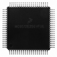
MC9S12E256VFUE Freescale Semiconductor, MC9S12E256VFUE Datasheet - Page 339

MC9S12E256VFUE
Manufacturer Part Number
MC9S12E256VFUE
Description
IC MCU 256K FLASH 25MHZ 80-QFP
Manufacturer
Freescale Semiconductor
Series
HCS12r
Datasheet
1.MC9S12E256CFUE.pdf
(602 pages)
Specifications of MC9S12E256VFUE
Core Processor
HCS12
Core Size
16-Bit
Speed
25MHz
Connectivity
EBI/EMI, I²C, SCI, SPI
Peripherals
POR, PWM, WDT
Number Of I /o
60
Program Memory Size
256KB (256K x 8)
Program Memory Type
FLASH
Ram Size
16K x 8
Voltage - Supply (vcc/vdd)
2.35 V ~ 2.75 V
Data Converters
A/D 16x10b; D/A 2x8b
Oscillator Type
Internal
Operating Temperature
-40°C ~ 105°C
Package / Case
80-QFP
Processor Series
S12E
Core
HCS12
Data Bus Width
16 bit
Data Ram Size
16 KB
Interface Type
I2C, SCI, SPI
Maximum Clock Frequency
50 MHz
Number Of Programmable I/os
60
Number Of Timers
12
Maximum Operating Temperature
+ 105 C
Mounting Style
SMD/SMT
3rd Party Development Tools
EWHCS12
Minimum Operating Temperature
- 40 C
On-chip Adc
10 bit, 16 Channel
On-chip Dac
8 bit, 2 Channel
Package
80PQFP
Family Name
HCS12
Maximum Speed
50 MHz
For Use With
M68EVB912E128 - BOARD EVAL FOR MC9S12E128/64
Lead Free Status / RoHS Status
Lead free / RoHS Compliant
Eeprom Size
-
Lead Free Status / Rohs Status
Details
Available stocks
Company
Part Number
Manufacturer
Quantity
Price
Company:
Part Number:
MC9S12E256VFUE
Manufacturer:
Freescale Semiconductor
Quantity:
10 000
- Current page: 339 of 602
- Download datasheet (4Mb)
11.3.2.16 PMF Value 2 Register (PMFVAL2)
Read and write anytime.
11.3.2.17 PMF Value 3 Register (PMFVAL3)
Read and write anytime.
Freescale Semiconductor
Module Base + 0x0014
Module Base + 0x0016
PMFVAL2
PMFVAL3
Reset
Reset
Field
Field
16–0
16–0
W
W
R
R
15
15
0
0
PMF Value 2 Bits — The 16-bit signed value in this buffered register is the pulse width in PWM2 clock period.
A value less than or equal to zero deactivates the PWM output for the entire PWM period. A value greater than,
or equal to the modulus, activates the PWM output for the entire PWM period. See
activate and deactivate refer to the high and low logic states of the PWM output.
Note: PMFVAL2 is buffered. The value written does not take effect until the LDOK bit is set and the next PWM
PMF Value 3 Bits — The 16-bit signed value in this buffered register is the pulse width in PWM3 clock period.
A value less than or equal to zero deactivates the PWM output for the entire PWM period. A value greater than,
or equal to the modulus, activates the PWM output for the entire PWM period. See
activate and deactivate refer to the high and low logic states of the PWM output.
Note: PMFVAL3 is buffered. The value written does not take effect until the LDOK bit is set and the next PWM
14
14
0
0
load cycle begins. Reading PMFVAL2 reads the value in the buffer and not necessarily the value the PWM
generator is currently using.
load cycle begins. Reading PMFVAL3 reads the value in the buffer and not necessarily the value the PWM
generator is currently using.
13
13
0
0
12
12
0
0
Figure 11-22. PMF Value 2 Register (PMFVAL2)
Figure 11-23. PMF Value 3 Register (PMFVAL3)
Table 11-21. PMFVAL2 Field Descriptions
Table 11-22. PMFVAL3 Field Descriptions
11
11
0
0
MC9S12E256 Data Sheet, Rev. 1.08
10
10
0
0
0
0
9
9
Chapter 11 Pulse Width Modulator with Fault Protection (PMF15B6CV2)
PMFVAL2
PMFVAL3
0
0
8
8
Description
Description
0
0
7
7
0
0
6
6
0
0
5
5
4
0
4
0
Table
Table
0
0
3
3
11-46. The terms
11-46. The terms
0
0
2
2
0
0
1
1
0
0
0
0
339
Related parts for MC9S12E256VFUE
Image
Part Number
Description
Manufacturer
Datasheet
Request
R
Part Number:
Description:
Manufacturer:
Freescale Semiconductor, Inc
Datasheet:
Part Number:
Description:
Manufacturer:
Freescale Semiconductor, Inc
Datasheet:
Part Number:
Description:
Manufacturer:
Freescale Semiconductor, Inc
Datasheet:
Part Number:
Description:
Manufacturer:
Freescale Semiconductor, Inc
Datasheet:
Part Number:
Description:
Manufacturer:
Freescale Semiconductor, Inc
Datasheet:
Part Number:
Description:
Manufacturer:
Freescale Semiconductor, Inc
Datasheet:
Part Number:
Description:
Manufacturer:
Freescale Semiconductor, Inc
Datasheet:
Part Number:
Description:
Manufacturer:
Freescale Semiconductor, Inc
Datasheet:
Part Number:
Description:
Manufacturer:
Freescale Semiconductor, Inc
Datasheet:
Part Number:
Description:
Manufacturer:
Freescale Semiconductor, Inc
Datasheet:
Part Number:
Description:
Manufacturer:
Freescale Semiconductor, Inc
Datasheet:
Part Number:
Description:
Manufacturer:
Freescale Semiconductor, Inc
Datasheet:
Part Number:
Description:
Manufacturer:
Freescale Semiconductor, Inc
Datasheet:
Part Number:
Description:
Manufacturer:
Freescale Semiconductor, Inc
Datasheet:
Part Number:
Description:
Manufacturer:
Freescale Semiconductor, Inc
Datasheet:


