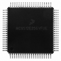
MC9S12E256VFUE Freescale Semiconductor, MC9S12E256VFUE Datasheet - Page 447

MC9S12E256VFUE
Manufacturer Part Number
MC9S12E256VFUE
Description
IC MCU 256K FLASH 25MHZ 80-QFP
Manufacturer
Freescale Semiconductor
Series
HCS12r
Datasheet
1.MC9S12E256CFUE.pdf
(602 pages)
Specifications of MC9S12E256VFUE
Core Processor
HCS12
Core Size
16-Bit
Speed
25MHz
Connectivity
EBI/EMI, I²C, SCI, SPI
Peripherals
POR, PWM, WDT
Number Of I /o
60
Program Memory Size
256KB (256K x 8)
Program Memory Type
FLASH
Ram Size
16K x 8
Voltage - Supply (vcc/vdd)
2.35 V ~ 2.75 V
Data Converters
A/D 16x10b; D/A 2x8b
Oscillator Type
Internal
Operating Temperature
-40°C ~ 105°C
Package / Case
80-QFP
Processor Series
S12E
Core
HCS12
Data Bus Width
16 bit
Data Ram Size
16 KB
Interface Type
I2C, SCI, SPI
Maximum Clock Frequency
50 MHz
Number Of Programmable I/os
60
Number Of Timers
12
Maximum Operating Temperature
+ 105 C
Mounting Style
SMD/SMT
3rd Party Development Tools
EWHCS12
Minimum Operating Temperature
- 40 C
On-chip Adc
10 bit, 16 Channel
On-chip Dac
8 bit, 2 Channel
Package
80PQFP
Family Name
HCS12
Maximum Speed
50 MHz
For Use With
M68EVB912E128 - BOARD EVAL FOR MC9S12E128/64
Lead Free Status / RoHS Status
Lead free / RoHS Compliant
Eeprom Size
-
Lead Free Status / Rohs Status
Details
Available stocks
Company
Part Number
Manufacturer
Quantity
Price
Company:
Part Number:
MC9S12E256VFUE
Manufacturer:
Freescale Semiconductor
Quantity:
10 000
- Current page: 447 of 602
- Download datasheet (4Mb)
15.1.2.2
If the part is in secure mode, the operation of the BDM is reduced to a small subset of its regular run mode
operation. Secure operation prevents access to FLASH or EEPROM other than allowing erasure.
15.2
A single-wire interface pin is used to communicate with the BDM system. Two additional pins are used
for instruction tagging. These pins are part of the multiplexed external bus interface (MEBI) sub-block and
all interfacing between the MEBI and BDM is done within the core interface boundary. Functional
descriptions of the pins are provided below for completeness.
15.2.1
Debugging control logic communicates with external devices serially via the single-wire background
interface pin (BKGD). During reset, this pin is a mode select input which selects between normal and
special modes of operation. After reset, this pin becomes the dedicated serial interface pin for the
background debug mode.
15.2.2
This pin is used to tag the high byte of an instruction. When instruction tagging is on, a logic 0 at the falling
edge of the external clock (ECLK) tags the high half of the instruction word being read into the instruction
queue.
15.2.3
This pin is used to tag the low byte of an instruction. When instruction tagging is on and low strobe is
enabled, a logic 0 at the falling edge of the external clock (ECLK) tags the low half of the instruction word
being read into the instruction queue.
Freescale Semiconductor
•
•
•
•
•
BKGD — Background interface pin
TAGHI — High byte instruction tagging pin
TAGLO — Low byte instruction tagging pin
BKGD and TAGHI share the same pin.
TAGLO and LSTRB share the same pin.
External Signal Description
BKGD — Background Interface Pin
TAGHI — High Byte Instruction Tagging Pin
TAGLO — Low Byte Instruction Tagging Pin
Secure Mode Operation
Generally these pins are shared as described, but it is best to check
Chapter 1, “MC9S12E256 Device Overview (MC9S12E256DGV1)”
make certain. All MCUs at the time of this writing have followed this pin
sharing scheme.
MC9S12E256 Data Sheet, Rev. 1.08
NOTE
Chapter 15 Background Debug Module (BDMV4)
to
447
Related parts for MC9S12E256VFUE
Image
Part Number
Description
Manufacturer
Datasheet
Request
R
Part Number:
Description:
Manufacturer:
Freescale Semiconductor, Inc
Datasheet:
Part Number:
Description:
Manufacturer:
Freescale Semiconductor, Inc
Datasheet:
Part Number:
Description:
Manufacturer:
Freescale Semiconductor, Inc
Datasheet:
Part Number:
Description:
Manufacturer:
Freescale Semiconductor, Inc
Datasheet:
Part Number:
Description:
Manufacturer:
Freescale Semiconductor, Inc
Datasheet:
Part Number:
Description:
Manufacturer:
Freescale Semiconductor, Inc
Datasheet:
Part Number:
Description:
Manufacturer:
Freescale Semiconductor, Inc
Datasheet:
Part Number:
Description:
Manufacturer:
Freescale Semiconductor, Inc
Datasheet:
Part Number:
Description:
Manufacturer:
Freescale Semiconductor, Inc
Datasheet:
Part Number:
Description:
Manufacturer:
Freescale Semiconductor, Inc
Datasheet:
Part Number:
Description:
Manufacturer:
Freescale Semiconductor, Inc
Datasheet:
Part Number:
Description:
Manufacturer:
Freescale Semiconductor, Inc
Datasheet:
Part Number:
Description:
Manufacturer:
Freescale Semiconductor, Inc
Datasheet:
Part Number:
Description:
Manufacturer:
Freescale Semiconductor, Inc
Datasheet:
Part Number:
Description:
Manufacturer:
Freescale Semiconductor, Inc
Datasheet:


