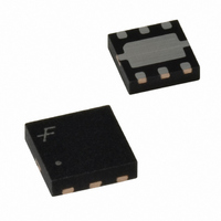
FAN2558MP15X Fairchild Semiconductor, FAN2558MP15X Datasheet - Page 7

FAN2558MP15X
Manufacturer Part Number
FAN2558MP15X
Description
IC REG LDO 180MA 1.5V 2X2 6MLP
Manufacturer
Fairchild Semiconductor
Datasheet
1.FAN2558S33X.pdf
(15 pages)
Specifications of FAN2558MP15X
Regulator Topology
Positive Fixed
Voltage - Output
1.5V
Voltage - Input
2.7 ~ 5.5 V
Number Of Regulators
1
Current - Output
180mA (Max)
Current - Limit (min)
260mA
Operating Temperature
-40°C ~ 85°C
Mounting Type
Surface Mount
Package / Case
6-MLP
Number Of Outputs
1
Polarity
Positive
Input Voltage Max
5.5 V
Output Voltage
1.5 V
Output Type
Fixed
Dropout Voltage (max)
400 mV
Output Current
180 mA
Line Regulation
0.3 % / V
Load Regulation
2.5 %
Voltage Regulation Accuracy
1 %
Maximum Operating Temperature
+ 125 C
Mounting Style
SMD/SMT
Minimum Operating Temperature
- 40 C
Lead Free Status / RoHS Status
Lead free / RoHS Compliant
Voltage - Dropout (typical)
-
Lead Free Status / Rohs Status
Lead free / RoHS Compliant
Control Functions
Enable Pin
Connecting 2V or greater to the Enable pin will enable the
output, while 0.4V or less will disable it while reducing the
quiescent current consumption to less than 1µA. If this shut-
down function is not needed, the pin can simply be con-
nected permanently to the V
will cause erratic operation.
Error Flag (Power Good)
Fault conditions such as input voltage dropout (low V
overheating, or overloading (excessive output current), will
set an error flag. The PG pin which is an open-drain output,
will go LOW when V
output voltage. When the voltage at V
95% of the specified output voltage, the PG pin is HIGH. A
logic pull-up resistor of 47K is recommended at this out-
put. The pin can be left disconnected if unused.
Thermal Protection
The FAN2558/FAN2559 is designed to supply high peak
output currents for brief periods, however sustained exces-
sive output load at high input - output voltage difference will
increase the device’s temperature and exceed maximum rat-
ings due to power dissipation. During output overload condi-
tions, when the die temperature exceeds the shutdown limit
temperature of 150°C, an onboard thermal protection will
disable the output until the temperature drops approximately
10°C below the limit, at which point the output is re-enabled.
During a thermal shutdown, the user may assert the power-
down function at the Enable pin, reducing power consump-
tion to a minimum.
Thermal Characteristics
The FAN2558/FAN2559 is designed to supply 180mA at the
specified output voltage with an operating die (junction)
temperature of up to 125°C. Once the power dissipation and
thermal resistance is known, the maximum junction tempera-
ture of the device can be calculated. While the power dissipa-
tion is calculated from known electrical parameters, the
actual thermal resistance depends on the thermal characteris-
tics of the SOT23-5 surface-mount package and the sur-
rounding PC board copper to which it is mounted.
The power dissipation is equal to the product of the input-to-
output voltage differential and the output current plus the
ground current multiplied by the input voltage,
or:
REV. 1.0.4 3/15/04
PRODUCT SPECIFICATIONS
P
D
=
V
IN
–
V
OUT
OUT
I
OUT
is less than 95% or the specified
IN
+
pin. Allowing this pin to float
V
IN
OUT
I
GND
is greater than
IN
),
The ground pin current I
provided in the Electrical Characteristics section.
The relationship describing the thermal behavior of the
package is:
where T
ture of the die, which is 125°C, and T
ing temperature.
board layout and can be empirically obtained. While the
(junction-to-case) of the SOT23-5 package is specified at
130°C /W, the
least 235°C /W. This can be improved by providing a heat
sink of surrounding copper ground on the PWB. Depending
on the size of the copper area, the resulting
from approximately 180°C /W for one square inch to nearly
130°C /W for 4 square inches. The addition of backside cop-
per with through-holes, stiffeners, and other enhancements
can also aid in reducing thermal resistance. The heat contrib-
uted by the dissipation of other devices located nearby must
be included in the design considerations. Once the limiting
parameters in these two relationships have been determined,
the design can be modified to ensure that the device remains
within specified operating conditions. If overload conditions
are not considered, it is possible for the device to enter a
thermal cycling loop, in which the circuit enters a shutdown
condition, cools, re-enables, and then again overheats and
shuts down repeatedly due to an unmanaged fault condition.
Adjustable Version
The FAN2558ADJ includes an input pin ADJ which allows
the user to select an output voltage ranging from 1V to near
V
sented to the ADJ pin is fed to the onboard error amplifier
which adjusts the output voltage until V
onboard bandgap reference voltage of 1.00V(typ). The equa-
tion is:
Since the bandgap reference voltage is trimmed, 1% initial
accuracy can be achieved. The total value of the resistor
chain should not exceed 250KOhm total to keep the error
amplifier biased during no-load conditions. Programming
output voltages very near V
tude and variation of the dropout voltage V
ply, and temperature variations. Note that the low-leakage
FET input to the CMOS error amplifier induces no bias
current error to the calculation.
IN
, using an external resistor divider. The voltage V
J(max)
is the maximum allowable junction tempera-
JA
P
V
JA
of the minimum PWB footprint will be at
D max
OUT
is dependent on the surrounding PC
=
GND
=
0.59V
IN
can be found in the charts
T
-------------------------------
need to allow for the magni-
J max
JA
1
A
–
+
T
is the ambient operat-
R
----- -
R
ADJ
A
1
2
DO
FAN2558/FAN2559
is equal to the
JA
over load, sup-
can range
ADJ
pre-
JC
7


