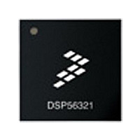
XC56309VL100A Freescale Semiconductor, XC56309VL100A Datasheet - Page 153

XC56309VL100A
Manufacturer Part Number
XC56309VL100A
Description
IC DSP 24BIT 100MHZ 196-MAPBGA
Manufacturer
Freescale Semiconductor
Series
DSP563xxr
Type
Fixed Pointr
Specifications of XC56309VL100A
Interface
Host Interface, SSI, SCI
Clock Rate
100MHz
Non-volatile Memory
ROM (576 B)
On-chip Ram
24kB
Voltage - I/o
3.30V
Voltage - Core
3.30V
Operating Temperature
-40°C ~ 100°C
Mounting Type
Surface Mount
Package / Case
196-MAPBGA
Device Core Size
24b
Format
Fixed Point
Clock Freq (max)
100MHz
Mips
100
Device Input Clock Speed
100MHz
Ram Size
102KB
Operating Supply Voltage (typ)
3.3V
Operating Supply Voltage (min)
3V
Operating Supply Voltage (max)
3.6V
Operating Temp Range
-40C to 100C
Operating Temperature Classification
Industrial
Mounting
Surface Mount
Pin Count
196
Package Type
MA-BGA
Lead Free Status / RoHS Status
Lead free / RoHS Compliant
Available stocks
Company
Part Number
Manufacturer
Quantity
Price
Company:
Part Number:
XC56309VL100A
Manufacturer:
Freescale Semiconductor
Quantity:
10 000
Company:
Part Number:
XC56309VL100AR2
Manufacturer:
Freescale Semiconductor
Quantity:
10 000
- Current page: 153 of 284
- Download datasheet (4Mb)
Freescale Semiconductor
Bit Number
8–7
9
6
5
4
Table 7-4. ESSI Control Register B (CRB) Bit Definitions (Continued)
Bit Name
FSL[1–0]
SCKD
SHFD
SCD2
FSR
Reset Value
0
0
0
0
0
DSP56309 User’s Manual, Rev. 1
Frame Sync Relative Timing
Determines the relative timing of the receive and transmit frame sync signal
in reference to the serial data lines for word length frame sync only. When
FSR is cleared, the word length frame sync occurs together with the first bit
of the data word of the first slot. When FSR is set, the word length frame
sync occurs one serial clock cycle earlier (that is, simultaneously with the
last bit of the previous data word).
Frame Sync Length
Selects the length of frame sync to be generated or recognized, as in
Figure 7-6 on page -23, Figure 7-9 on page -26, and Figure 7-10, Network
Mode, External Frame Sync (8 Bit, 2 Words in Frame), on page 7-26.
Shift Direction
Determines the shift direction of the transmit or receive shift register. If
SHFD is set, data is shifted in and out with the LSB first. If SHFD is cleared,
data is shifted in and out with the MSB first, as in Figure 7-12, ESSI Data
Path Programming Model (SHFD = 0), on page 7-29 and Figure 7-13 on
page -30.
Clock Source Direction
Selects the source of the clock signal that clocks the transmit shift register
in Asynchronous mode and both the transmit and receive shift registers in
Synchronous mode. If SCKD is set and the ESSI is in Synchronous mode,
the internal clock is the source of the clock signal used for all the transmit
shift registers and the receive shift register. If SCKD is set and the ESSI is
in Asynchronous mode, the internal clock source becomes the bit clock for
the transmit shift register and word length divider. The internal clock is
output on the SCK signal. When SCKD is cleared, the external clock source
is selected. The internal clock generator is disconnected from the SCK
signal, and an external clock source may drive this signal.
Serial Control Direction 2
Controls the direction of the SC2 I/O signal. When SCD2 is set, SC2 is an
output; when SCD2 is cleared, SC2 is an input.
Note:
FSL1
0
0
1
1
Programming the ESSI to use an internal frame sync (that is,
SCD2 = 1 in CRB) causes the SC2 and SC1 signals to be
programmed as outputs. However, if the corresponding
multiplexed pins are programmed by the Port Control Register
(PCR) to be GPIOs, the GPIO Port Direction Register (PRR)
chooses their direction. The ESSI uses an external frame sync if
GPIO is selected. To assure correct operation, either program the
GPIO pins as outputs or configure the pins in the PCR as ESSI
signals. The default selection for these signals after reset is GPIO.
This note applies to both ESSI0 and ESSI1.
FSL0
0
1
0
1
Description
word
word
RX
bit
bit
Frame Sync Length
ESSI Programming Model
word
word
TX
bit
bit
7-21
Related parts for XC56309VL100A
Image
Part Number
Description
Manufacturer
Datasheet
Request
R
Part Number:
Description:
Manufacturer:
Freescale Semiconductor, Inc
Datasheet:
Part Number:
Description:
Manufacturer:
Freescale Semiconductor, Inc
Datasheet:
Part Number:
Description:
Manufacturer:
Freescale Semiconductor, Inc
Datasheet:
Part Number:
Description:
Manufacturer:
Freescale Semiconductor, Inc
Datasheet:
Part Number:
Description:
Manufacturer:
Freescale Semiconductor, Inc
Datasheet:
Part Number:
Description:
Manufacturer:
Freescale Semiconductor, Inc
Datasheet:
Part Number:
Description:
Manufacturer:
Freescale Semiconductor, Inc
Datasheet:
Part Number:
Description:
Manufacturer:
Freescale Semiconductor, Inc
Datasheet:
Part Number:
Description:
Manufacturer:
Freescale Semiconductor, Inc
Datasheet:
Part Number:
Description:
Manufacturer:
Freescale Semiconductor, Inc
Datasheet:
Part Number:
Description:
Manufacturer:
Freescale Semiconductor, Inc
Datasheet:
Part Number:
Description:
Manufacturer:
Freescale Semiconductor, Inc
Datasheet:
Part Number:
Description:
Manufacturer:
Freescale Semiconductor, Inc
Datasheet:
Part Number:
Description:
Manufacturer:
Freescale Semiconductor, Inc
Datasheet:
Part Number:
Description:
Manufacturer:
Freescale Semiconductor, Inc
Datasheet:


