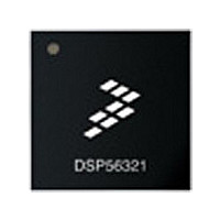
XC56309VL100A Freescale Semiconductor, XC56309VL100A Datasheet - Page 98

XC56309VL100A
Manufacturer Part Number
XC56309VL100A
Description
IC DSP 24BIT 100MHZ 196-MAPBGA
Manufacturer
Freescale Semiconductor
Series
DSP563xxr
Type
Fixed Pointr
Specifications of XC56309VL100A
Interface
Host Interface, SSI, SCI
Clock Rate
100MHz
Non-volatile Memory
ROM (576 B)
On-chip Ram
24kB
Voltage - I/o
3.30V
Voltage - Core
3.30V
Operating Temperature
-40°C ~ 100°C
Mounting Type
Surface Mount
Package / Case
196-MAPBGA
Device Core Size
24b
Format
Fixed Point
Clock Freq (max)
100MHz
Mips
100
Device Input Clock Speed
100MHz
Ram Size
102KB
Operating Supply Voltage (typ)
3.3V
Operating Supply Voltage (min)
3V
Operating Supply Voltage (max)
3.6V
Operating Temp Range
-40C to 100C
Operating Temperature Classification
Industrial
Mounting
Surface Mount
Pin Count
196
Package Type
MA-BGA
Lead Free Status / RoHS Status
Lead free / RoHS Compliant
Available stocks
Company
Part Number
Manufacturer
Quantity
Price
Company:
Part Number:
XC56309VL100A
Manufacturer:
Freescale Semiconductor
Quantity:
10 000
Company:
Part Number:
XC56309VL100AR2
Manufacturer:
Freescale Semiconductor
Quantity:
10 000
- Current page: 98 of 284
- Download datasheet (4Mb)
Programming the Peripherals
5.5 General-Purpose Input/Output (GPIO)
The DSP56309 provides 34 bidirectional signals that can be configured as GPIO signals or as
peripheral dedicated signals. No dedicated GPIO signals are provided. All of these signals are
GPIO by default after reset. The control register settings of the DSP56309 peripherals determine
whether these signals function as GPIO or as peripheral dedicated signals. This section describes
how signals can be used as GPIO.
Chapter 2, Signals/Connections details the special uses of the 34 bidirectional signals. These
signals fall into five groups and are controlled separately or as a group:
5.5.1 Port B Signals and Registers
Each of the 16 Port B signals not used as an HI08 signal can be configured as a GPIO signal.
Three registers control the GPIO functionality of Port B: host control register (HCR), host port
GPIO data register (HDR), and host port GPIO direction register (HDDR). Chapter 6, Host
Interface (HI08), discusses these registers.
5-6
Port B: 16 GPIO signals (shared with the HI08 signals)
Port C: six GPIO signals (shared with the ESSI0 signals)
Port D: six GPIO signals (shared with the ESSI1 signals)
Port E: three GPIO signals (shared with the SCI signals)
Timers: three GPIO signals (shared with the triple timer signals)
Host Interface
(HI08) Port
DSP56309
Figure 5-2. Port B Signals
DSP56309 User’s Manual, Rev. 1
Non-Multiplexed
Bus
H[0–7]
HA0
HA1
HA2
HCS/HCS
Single DS
HRW
HDS/HDS
Single HR
HREQ/HREQ
HACK/HACK
HAS/HAS
HA8
HA9
HA10
Double DS
HRD/HRD
HWR/HWR
Double HR
HTRQ/HTRQ
Multiplexed
Bus
HAD[0–7]
HRRQ/HRRQ
Port B GPIO
PB[0–7]
PB8
PB9
PB10
PB13
PB11
PB12
PB14
PB15
Freescale Semiconductor
Related parts for XC56309VL100A
Image
Part Number
Description
Manufacturer
Datasheet
Request
R
Part Number:
Description:
Manufacturer:
Freescale Semiconductor, Inc
Datasheet:
Part Number:
Description:
Manufacturer:
Freescale Semiconductor, Inc
Datasheet:
Part Number:
Description:
Manufacturer:
Freescale Semiconductor, Inc
Datasheet:
Part Number:
Description:
Manufacturer:
Freescale Semiconductor, Inc
Datasheet:
Part Number:
Description:
Manufacturer:
Freescale Semiconductor, Inc
Datasheet:
Part Number:
Description:
Manufacturer:
Freescale Semiconductor, Inc
Datasheet:
Part Number:
Description:
Manufacturer:
Freescale Semiconductor, Inc
Datasheet:
Part Number:
Description:
Manufacturer:
Freescale Semiconductor, Inc
Datasheet:
Part Number:
Description:
Manufacturer:
Freescale Semiconductor, Inc
Datasheet:
Part Number:
Description:
Manufacturer:
Freescale Semiconductor, Inc
Datasheet:
Part Number:
Description:
Manufacturer:
Freescale Semiconductor, Inc
Datasheet:
Part Number:
Description:
Manufacturer:
Freescale Semiconductor, Inc
Datasheet:
Part Number:
Description:
Manufacturer:
Freescale Semiconductor, Inc
Datasheet:
Part Number:
Description:
Manufacturer:
Freescale Semiconductor, Inc
Datasheet:
Part Number:
Description:
Manufacturer:
Freescale Semiconductor, Inc
Datasheet:


