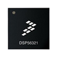
XC56309VL100A Freescale Semiconductor, XC56309VL100A Datasheet - Page 70

XC56309VL100A
Manufacturer Part Number
XC56309VL100A
Description
IC DSP 24BIT 100MHZ 196-MAPBGA
Manufacturer
Freescale Semiconductor
Series
DSP563xxr
Type
Fixed Pointr
Specifications of XC56309VL100A
Interface
Host Interface, SSI, SCI
Clock Rate
100MHz
Non-volatile Memory
ROM (576 B)
On-chip Ram
24kB
Voltage - I/o
3.30V
Voltage - Core
3.30V
Operating Temperature
-40°C ~ 100°C
Mounting Type
Surface Mount
Package / Case
196-MAPBGA
Device Core Size
24b
Format
Fixed Point
Clock Freq (max)
100MHz
Mips
100
Device Input Clock Speed
100MHz
Ram Size
102KB
Operating Supply Voltage (typ)
3.3V
Operating Supply Voltage (min)
3V
Operating Supply Voltage (max)
3.6V
Operating Temp Range
-40C to 100C
Operating Temperature Classification
Industrial
Mounting
Surface Mount
Pin Count
196
Package Type
MA-BGA
Lead Free Status / RoHS Status
Lead free / RoHS Compliant
Available stocks
Company
Part Number
Manufacturer
Quantity
Price
Company:
Part Number:
XC56309VL100A
Manufacturer:
Freescale Semiconductor
Quantity:
10 000
Company:
Part Number:
XC56309VL100AR2
Manufacturer:
Freescale Semiconductor
Quantity:
10 000
- Current page: 70 of 284
- Download datasheet (4Mb)
Reset:
Core Configuration
4.3.2 Operating Mode Register (OMR)
The OMR is a read/write register divided into three byte-sized units. The lowest two bytes (EOM
and COM) control the chip’s operating mode. The high byte (SCS) controls and monitors the
stack extension. The OMR control bits are shown in Figure 4-2.
The Enhanced Operating Mode (EOM) and Chip Operating Mode (COM) bytes are affected only
by processor reset and by instructions directly referencing the OMR (that is, ANDI, ORI, and
other instructions, such as MOVEC, that specify OMR as a destination). The Stack
Control/Status (SCS) byte is referenced implicitly by some instructions, such as DO, JSR, and
RTI, or directly by the MOVEC instruction. During processor reset, the chip operating mode bits
(MD, MC, MB, and MA) are loaded from the external mode select pins MODD, MODC,
MODB, and MODA respectively. Table 4-3 defines the DSP56309 OMR bits.
4-12
23
0
*
Bit Number
23–21
respectively).
After reset, these bits reflect the corresponding value of the mode input (that is, MODD, MODC, MODB, or MODA,
Reserved bit. Read as zero; write to zero for future compatibility
22
Stack Control/Status (SCS)
20
19
18
0
21
0
SEN WRP EOV EUN XYS ATE APD ABE BRT TAS BE CDP[1–0] MS
20
0
Bit Name
WRP
SEN
EOV
19
0
Table 4-3. Operating Mode Register (OMR) Bit Definitions
18
0
Figure 4-2. Operating Mode Register (OMR)
Reset Value
17
0
16
0
0
0
0
0
15
0
DSP56309 User’s Manual, Rev. 1
Extended Operating Mode (EOM)
Reserved. Write to 0 for future compatibility.
Stack Extension Enable
Enables/disables the stack extension in data memory. If the SEN bit is set,
the extension is enabled. Hardware reset clears this bit, so the default out of
reset is a disabled stack extension.
Stack Extension Wrap Flag
Set when copying from the internal hardware stack (System Stack Register
file) to the stack extension memory begins. You can use this flag during the
debugging phase of the software development to evaluate and increase the
speed of software-implemented algorithms. The WRP flag is a sticky bit (that
is, cleared only by hardware reset or by an explicit MOVEC operation to the
OMR).
Stack Extension Overflow Flag
Set when a stack overflow occurs in Stack Extended mode. Extended stack
overflow is recognized when a push operation is requested while SP = SZ
(Stack Size register), and the Extended mode is enabled by the SEN bit. The
EOV flag is a sticky bit (that is, cleared only by hardware reset or by an
explicit MOVEC operation to the OMR). The transition of the EOV flag from
zero to one causes a Priority Level 3 (Non-maskable) stack error exception.
14
0
13
0
12
0
11
0
10
0
9
1
Description
8
1
7
0
Chip Operating Mode (COM)
SD
6
0
5
0
Freescale Semiconductor
EBD MD MC MB MA
4
0
3
*
2
*
1
*
0
*
Related parts for XC56309VL100A
Image
Part Number
Description
Manufacturer
Datasheet
Request
R
Part Number:
Description:
Manufacturer:
Freescale Semiconductor, Inc
Datasheet:
Part Number:
Description:
Manufacturer:
Freescale Semiconductor, Inc
Datasheet:
Part Number:
Description:
Manufacturer:
Freescale Semiconductor, Inc
Datasheet:
Part Number:
Description:
Manufacturer:
Freescale Semiconductor, Inc
Datasheet:
Part Number:
Description:
Manufacturer:
Freescale Semiconductor, Inc
Datasheet:
Part Number:
Description:
Manufacturer:
Freescale Semiconductor, Inc
Datasheet:
Part Number:
Description:
Manufacturer:
Freescale Semiconductor, Inc
Datasheet:
Part Number:
Description:
Manufacturer:
Freescale Semiconductor, Inc
Datasheet:
Part Number:
Description:
Manufacturer:
Freescale Semiconductor, Inc
Datasheet:
Part Number:
Description:
Manufacturer:
Freescale Semiconductor, Inc
Datasheet:
Part Number:
Description:
Manufacturer:
Freescale Semiconductor, Inc
Datasheet:
Part Number:
Description:
Manufacturer:
Freescale Semiconductor, Inc
Datasheet:
Part Number:
Description:
Manufacturer:
Freescale Semiconductor, Inc
Datasheet:
Part Number:
Description:
Manufacturer:
Freescale Semiconductor, Inc
Datasheet:
Part Number:
Description:
Manufacturer:
Freescale Semiconductor, Inc
Datasheet:


