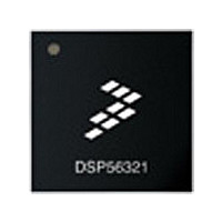
XC56309VL100A Freescale Semiconductor, XC56309VL100A Datasheet - Page 207

XC56309VL100A
Manufacturer Part Number
XC56309VL100A
Description
IC DSP 24BIT 100MHZ 196-MAPBGA
Manufacturer
Freescale Semiconductor
Series
DSP563xxr
Type
Fixed Pointr
Specifications of XC56309VL100A
Interface
Host Interface, SSI, SCI
Clock Rate
100MHz
Non-volatile Memory
ROM (576 B)
On-chip Ram
24kB
Voltage - I/o
3.30V
Voltage - Core
3.30V
Operating Temperature
-40°C ~ 100°C
Mounting Type
Surface Mount
Package / Case
196-MAPBGA
Device Core Size
24b
Format
Fixed Point
Clock Freq (max)
100MHz
Mips
100
Device Input Clock Speed
100MHz
Ram Size
102KB
Operating Supply Voltage (typ)
3.3V
Operating Supply Voltage (min)
3V
Operating Supply Voltage (max)
3.6V
Operating Temp Range
-40C to 100C
Operating Temperature Classification
Industrial
Mounting
Surface Mount
Pin Count
196
Package Type
MA-BGA
Lead Free Status / RoHS Status
Lead free / RoHS Compliant
Available stocks
Company
Part Number
Manufacturer
Quantity
Price
Company:
Part Number:
XC56309VL100A
Manufacturer:
Freescale Semiconductor
Quantity:
10 000
Company:
Part Number:
XC56309VL100AR2
Manufacturer:
Freescale Semiconductor
Quantity:
10 000
- Current page: 207 of 284
- Download datasheet (4Mb)
9.3.2.3 Measurement Capture (Mode 6)
In Mode 6, the timer counts the number of clocks that elapse between when the timer starts and
when an external signal is received. At the first appropriate transition of the external clock
detected on the
interrupt is generated. The counter halts. The contents of the counter are loaded into the TCR.
The value of the TCR represents the delay between the setting of the TCSR[TE] bit and the
detection of the first clock edge signal on the
whether a high-to-low (1 to 0) or low-to-high (0 to 1) transition of the external clock signals the
end of the timing period. If the INV bit is set, a high-to-low transition signals the end of the
timing period. If INV is cleared, a low-to-high transition signals the end of the timing period.
Freescale Semiconductor
TC3
0
TCF (Compare Interrupt if TCIE = 1)
Mode 6 (internal clock): TRM = 1
N = write preload
M = write compare
TE
Clock
(CLK/2 or prescale CLK)
TLR
Counter
TCR
TIO pin
NOTE: If INV = 1, a 1-to-0 edge on TIO loads TCR with count and stops the counter.
TC2
Bit Settings
1
TIO
TC1
1
signal, TCSR[TCF] is set and, if the TCSR[TCIE] bit is set, a compare
Figure 9-15. Capture Measurement Mode, TRM = 0
TC0
N
0
0
Mode
delay being measured
first event
6
DSP56309 User’s Manual, Rev. 1
N
TIO
Capture
Name
signal. The value of the INV bit determines
N + 1
Mode Characteristics
Measurement
M
Function
M
N
Interrupt Service
reads TCR; delay
= M - N clock
periods
Counter stops
counting; overflow
may occur before
capture (TOF = 1)
Input
TIO
N + 1
Operating Modes
Internal
Clock
9-15
Related parts for XC56309VL100A
Image
Part Number
Description
Manufacturer
Datasheet
Request
R
Part Number:
Description:
Manufacturer:
Freescale Semiconductor, Inc
Datasheet:
Part Number:
Description:
Manufacturer:
Freescale Semiconductor, Inc
Datasheet:
Part Number:
Description:
Manufacturer:
Freescale Semiconductor, Inc
Datasheet:
Part Number:
Description:
Manufacturer:
Freescale Semiconductor, Inc
Datasheet:
Part Number:
Description:
Manufacturer:
Freescale Semiconductor, Inc
Datasheet:
Part Number:
Description:
Manufacturer:
Freescale Semiconductor, Inc
Datasheet:
Part Number:
Description:
Manufacturer:
Freescale Semiconductor, Inc
Datasheet:
Part Number:
Description:
Manufacturer:
Freescale Semiconductor, Inc
Datasheet:
Part Number:
Description:
Manufacturer:
Freescale Semiconductor, Inc
Datasheet:
Part Number:
Description:
Manufacturer:
Freescale Semiconductor, Inc
Datasheet:
Part Number:
Description:
Manufacturer:
Freescale Semiconductor, Inc
Datasheet:
Part Number:
Description:
Manufacturer:
Freescale Semiconductor, Inc
Datasheet:
Part Number:
Description:
Manufacturer:
Freescale Semiconductor, Inc
Datasheet:
Part Number:
Description:
Manufacturer:
Freescale Semiconductor, Inc
Datasheet:
Part Number:
Description:
Manufacturer:
Freescale Semiconductor, Inc
Datasheet:


