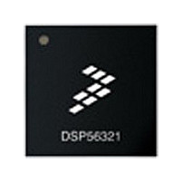
XC56309VL100A Freescale Semiconductor, XC56309VL100A Datasheet - Page 276

XC56309VL100A
Manufacturer Part Number
XC56309VL100A
Description
IC DSP 24BIT 100MHZ 196-MAPBGA
Manufacturer
Freescale Semiconductor
Series
DSP563xxr
Type
Fixed Pointr
Specifications of XC56309VL100A
Interface
Host Interface, SSI, SCI
Clock Rate
100MHz
Non-volatile Memory
ROM (576 B)
On-chip Ram
24kB
Voltage - I/o
3.30V
Voltage - Core
3.30V
Operating Temperature
-40°C ~ 100°C
Mounting Type
Surface Mount
Package / Case
196-MAPBGA
Device Core Size
24b
Format
Fixed Point
Clock Freq (max)
100MHz
Mips
100
Device Input Clock Speed
100MHz
Ram Size
102KB
Operating Supply Voltage (typ)
3.3V
Operating Supply Voltage (min)
3V
Operating Supply Voltage (max)
3.6V
Operating Temp Range
-40C to 100C
Operating Temperature Classification
Industrial
Mounting
Surface Mount
Pin Count
196
Package Type
MA-BGA
Lead Free Status / RoHS Status
Lead free / RoHS Compliant
Available stocks
Company
Part Number
Manufacturer
Quantity
Price
Company:
Part Number:
XC56309VL100A
Manufacturer:
Freescale Semiconductor
Quantity:
10 000
Company:
Part Number:
XC56309VL100AR2
Manufacturer:
Freescale Semiconductor
Quantity:
10 000
- Current page: 276 of 284
- Download datasheet (4Mb)
Index
Interrupt Mask (I) bits 4-10
Interrupt Priority Register Core (IPRC) 4-15
Interrupt Priority Register Peripherals (IPRP) 4-15
Interrupt Priority Register-Peripherals (IPR-P)
interrupt routines
Interrupt Service Routine (ISR) 7-8
interrupt trigger event 7-9
Interrupt Vector Register (IVR) 6-21
Inverter (INV) bit 9-25
IRQD–IRQA Priority and Mode (IDL–IAL) bits 4-15
J
Joint Test Action Group (JTAG) 1-8
L
Limit (L) bit 4-10
Loop Address register (LA) 1-8
Loop Counter register (LC) 1-8
M
M68HC11 SCI interface 8-14
manual conventions 1-2
mapping control registers 5-1
MC68000 family 6-26
MC68681 DUART 8-14
memory
Memory Expansion Port 1-5
memory map
Memory Switch mode 3-2
Memory Switch Mode (MS) bit 4-14
MODD, MODC, MODB, and MODA 8-7
mode control 2-8
Mode Register (MR) 4-7
Index-8
IRQD–IRQA Priority and Mode (IDL–IAL) 4-15
ESSI0 Interrupt Priority Level (S0L) 4-16
ESSI1 Interrupt Priority Level (S1L) 4-16
HI08 Interrupt Priority Level (HPL) 4-16
SCI Interrupt Priority Level (SCL) 4-16
Timer Interrupt Priority Level (TOL) 4-16
programming sheet B-12
Host Interface (HI08) 6-7
programming sheet B-22
Test Acces Port(TAP) 1-5
allocation switching 3-2
configuration 3-5
dynamic switching 3-5
expansion 3-1
external expansion port 1-9
maps 3-6
on-chip 1-9
internal I/O B-2
X data Memory 3-3
X data memory 3-4
,
9-27
,
,
9-4
2-20
,
4-34
DSP56309 User’s Manual, Rev. 1
,
4-16
Mode Select (MOD) bit 7-20
move (MOVE, MOVEP) instructions 5-1
MOVEP instruction 6-12
Multidrop mode 8-2
multiplexed bus mode 2-2
Multiplication Factor (MF) bits 4-21
Multiplier-Accumulator (MAC) 1-6
N
Negative (N) bit 4-11
Network mode 7-7
non-multiplexed bus mode 2-2
O
off-chip memory 1-5
On-Chip Emulation (OnCE) module 1-5
on-chip memory 1-5
On-Demand mode 7-9
operating frequency 1-5
operating mode 4-1
Operating Mode Register (OMR) 1-8
Overflow (V) bit 4-11
Overrun Error Flag (OR) bit 8-16
P
Parity Error (PE) bit 8-15
Peripheral I/O Expansion Bus 1-10
Do Loop Flag (LF) 4-9
Double-Precision Multiply Mode (DM) 4-9
Interrupt Mask (I) 4-10
Scaling (S) Mode 4-10
Sixteen-Bit Compatibility (SC) mode 4-9
Host Interface (HI08) 6-16
Address Attribute Priority Disable (APD) 4-13
Address Trace Enable (ATE) 4-13
Asynchronous Bus Arbitration Enable (ABE) 4-13
Bus Release Timing (BRT) 4-13
Cache Burst Mode Enable (BE) 4-14
Chip Operating Mode (MD–MA) 4-14
COM byte 4-12
Core-DMA Priority (CDP) 4-14
EOM byte 4-12
External Bus Disable (EBD) 4-14
Memory Switch Mode (MS) 4-14
programming sheet B-11
SCS byte 4-12
Stack Extension Enable (SEN) 4-12
Stack Extension Overflow Flag (EOV) 4-12
Stack Extension Underflow Flag (EUN) 4-13
Stack Extension Wrap Flag (WRP) 4-12
Stack Extension XY Select (XYS) 4-13
Stop Delay Mode (SD) 4-14
TA Synchronize Select (TAS) 4-13
,
,
1-9
3-1
,
7-14
,
6-3
,
,
6-3
6-15
Freescale Semiconductor
,
,
6-18
4-12
,
1-9
,
2-20
Related parts for XC56309VL100A
Image
Part Number
Description
Manufacturer
Datasheet
Request
R
Part Number:
Description:
Manufacturer:
Freescale Semiconductor, Inc
Datasheet:
Part Number:
Description:
Manufacturer:
Freescale Semiconductor, Inc
Datasheet:
Part Number:
Description:
Manufacturer:
Freescale Semiconductor, Inc
Datasheet:
Part Number:
Description:
Manufacturer:
Freescale Semiconductor, Inc
Datasheet:
Part Number:
Description:
Manufacturer:
Freescale Semiconductor, Inc
Datasheet:
Part Number:
Description:
Manufacturer:
Freescale Semiconductor, Inc
Datasheet:
Part Number:
Description:
Manufacturer:
Freescale Semiconductor, Inc
Datasheet:
Part Number:
Description:
Manufacturer:
Freescale Semiconductor, Inc
Datasheet:
Part Number:
Description:
Manufacturer:
Freescale Semiconductor, Inc
Datasheet:
Part Number:
Description:
Manufacturer:
Freescale Semiconductor, Inc
Datasheet:
Part Number:
Description:
Manufacturer:
Freescale Semiconductor, Inc
Datasheet:
Part Number:
Description:
Manufacturer:
Freescale Semiconductor, Inc
Datasheet:
Part Number:
Description:
Manufacturer:
Freescale Semiconductor, Inc
Datasheet:
Part Number:
Description:
Manufacturer:
Freescale Semiconductor, Inc
Datasheet:
Part Number:
Description:
Manufacturer:
Freescale Semiconductor, Inc
Datasheet:


