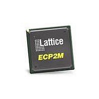
LFE2M20E-5FN256C Lattice, LFE2M20E-5FN256C Datasheet - Page 119

LFE2M20E-5FN256C
Manufacturer Part Number
LFE2M20E-5FN256C
Description
FPGA - Field Programmable Gate Array 19K LUTs 140 I/O SERDES DSP -5
Manufacturer
Lattice
Datasheet
1.LFE2-12SE-6FN256C.pdf
(389 pages)
Specifications of LFE2M20E-5FN256C
Number Of Macrocells
19000
Maximum Operating Frequency
311 MHz
Number Of Programmable I/os
140
Data Ram Size
1246208
Supply Voltage (max)
1.26 V
Maximum Operating Temperature
+ 85 C
Minimum Operating Temperature
0 C
Mounting Style
SMD/SMT
Supply Voltage (min)
1.14 V
Package / Case
FPBGA-256
Lead Free Status / RoHS Status
Lead free / RoHS Compliant
Available stocks
Company
Part Number
Manufacturer
Quantity
Price
Company:
Part Number:
LFE2M20E-5FN256C
Manufacturer:
Lattice Semiconductor Corporation
Quantity:
10 000
- Current page: 119 of 389
- Download datasheet (5Mb)
Lattice Semiconductor
LatticeECP2 Power Supply and NC
VCC
VCCIO0
VCCIO1
VCCIO2
VCCIO3
VCCIO4
VCCIO5
VCCIO6
VCCIO7
VCCIO8
VCCJ
VCCAUX
VCCPLL
GND
NC
1. All grounds must be electrically connected at the board level. For fpBGA packages, the total number of GND balls is less than the actual
2. NC pins should not be connected to any active signals, VCC or GND.
3. Pin orientation follows the conventional order from the pin 1 marking of the top side view and counter-clockwise.
4. Pin orientation A1 starts from the upper left corner of the top side view with alphabetical order ascending vertically and numerical order
Signals
number of GND logic connections from the die to the common package GND plane.
ascending horizontally.
2
1
16, 22, 29, 48, 54, 83,
94, 102, 128, 135
139
117
106
89
64
42
31
9
85
35
6, 39, 90, 142
None
11, 21, 30, 47, 51, 61,
81, 95, 105, 120, 133,
138
LFE2-6: 45, 46, 124,
127
LFE2-12: 127
144 TQFP
3
12, 19, 28, 40, 74, 80,
97, 116, 129, 140, 146,
171, 188, 198
195, 206
162, 170
143, 148
123, 135
93, 100
55, 63
38, 44
10, 14
113, 118
51
7, 30, 70, 86, 125, 151,
174, 190
None
5, 13, 17, 25, 32, 42, 60,
68, 77, 81, 89, 102, 115,
122, 139, 145, 159, 169,
175, 184, 192, 201
None
208 PQFP
3
4-16
LFE2-6: G7, G9, G10,
H7, J10, K10, K8
LFE2-12/LFE2-20: G7,
G9, G10, H7, J10, K10,
K8
C5, E7
C12, E10
E14, G12
K12, M14
M10, P12
M7, P5
K5, M3
E3, G5
T15
K7
G8, H10, J7, K9
None
A1, A16, B12, B5, C8,
E15, E2, H14, H8, H9,
J3, J8, J9, M15, M2, P9,
R12, R5, T1, T16
LFE2-6: K6, R3, P4
LFE2-12/LFE2-20:
None
256 fpBGA
LatticeECP2/M Family Data Sheet
4
LFE2-12/LFE2-20: N6, N18, J10,
J11, J12, J13, K14, K9, L14, L9,
M14, M9, N14, N9, P10, P11, P12,
P13
LFE2-35/LFE2-50: J10, J11, J12,
J13, K14, K9, L14, L9, M14, M9,
N14, N9, P10, P11, P12, P13
G10, G9, H8, H9
G11, G12, G13, G14
H14, H15, J15, K16
L16, M16, N16, P16
R14, T12, T13, T14
R9, T10, T11, T9
N7, P7, P8, R8
J8, K7, L7, M7
P15, R15
T8
G5, K5, R5, V7, V11, V8, V13,
V15, M17, P17, E17, G18, D11,
F13, C5, E6
LFE2-12/LFE2-20: None
LFE2-35: N6, N18
LFE2-50: N6, N18, K6, J16
A22, AA19, AA4, AB1, AB22, B19,
B4, C14, C9, D2, D21, F17, F6,
H10, H11, H12, H13, J14, J20, J3,
J9, K10, K11, K12, K13, K15, K8,
L10, L11, L12, L13, L15, L8, M10,
M11, M12, M13, M15, M8, N10,
N11, N12, N13, N15, N8, P14,
P20, P3, P9, R10, R11, R12, R13,
U17, U6, W2, W21, Y14, Y9, A1
LFE2-12: E3, F3, F1, H4, F2, H5,
G1, G3, G2, G4, K6, N1, M2, N2,
M1, N3, N5, N4, P5, N19, M19,
J22, L22, H22, K22, J16, D22, F21,
E21, E22, H19, G20, G19, F20,
C21, C22, H6, J6, H3, H2, H17,
H16, H20, H18
LFE2-20/LFE2-35: K6, J16, H6,
J6, H3, H2, H17, H16, H20, H18
LFE2-50: None
Pinout Information
484 fpBGA
4
Related parts for LFE2M20E-5FN256C
Image
Part Number
Description
Manufacturer
Datasheet
Request
R

Part Number:
Description:
FPGA - Field Programmable Gate Array 19K LUTs 304 I/O SERDES DSP -5
Manufacturer:
Lattice
Datasheet:

Part Number:
Description:
FPGA - Field Programmable Gate Array 19K LUTs 304 I/O SERDES DSP -5
Manufacturer:
Lattice

Part Number:
Description:
FPGA - Field Programmable Gate Array 19K LUTs 304 I/O SERDES DSP -6
Manufacturer:
Lattice
Datasheet:

Part Number:
Description:
FPGA - Field Programmable Gate Array 19K LUTs 140 I/O SERDES DSP -6
Manufacturer:
Lattice
Datasheet:
Part Number:
Description:
FPGA LatticeECP2M Family 19000 Cells 90nm (CMOS) Technology 1.2V 484-Pin FBGA
Manufacturer:
LATTICE SEMICONDUCTOR
Datasheet:
Part Number:
Description:
FPGA LatticeECP2M Family 19000 Cells 90nm (CMOS) Technology 1.2V 256-Pin FBGA
Manufacturer:
LATTICE SEMICONDUCTOR
Datasheet:
Part Number:
Description:
FPGA LatticeECP2M Family 19000 Cells 90nm (CMOS) Technology 1.2V 256-Pin FBGA
Manufacturer:
LATTICE SEMICONDUCTOR
Datasheet:

Part Number:
Description:
IC FPGA 20KLUTS 140I/O 256-BGA
Manufacturer:
Lattice
Datasheet:

Part Number:
Description:
IC FPGA 20KLUTS 140I/O 256-BGA
Manufacturer:
Lattice
Datasheet:

Part Number:
Description:
IC FPGA 20KLUTS 140I/O 256-BGA
Manufacturer:
Lattice
Datasheet:

Part Number:
Description:
IC FPGA 20KLUTS 304I/O 484-BGA
Manufacturer:
Lattice
Datasheet:

Part Number:
Description:
IC FPGA 20KLUTS 140I/O 256-BGA
Manufacturer:
Lattice
Datasheet:

Part Number:
Description:
IC FPGA 20KLUTS 140I/O 256-BGA
Manufacturer:
Lattice
Datasheet:

Part Number:
Description:
IC FPGA 20KLUTS 304I/O 484-BGA
Manufacturer:
Lattice
Datasheet:


