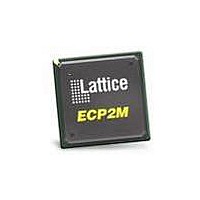
LFE2M20E-5FN256C Lattice, LFE2M20E-5FN256C Datasheet - Page 53

LFE2M20E-5FN256C
Manufacturer Part Number
LFE2M20E-5FN256C
Description
FPGA - Field Programmable Gate Array 19K LUTs 140 I/O SERDES DSP -5
Manufacturer
Lattice
Datasheet
1.LFE2-12SE-6FN256C.pdf
(389 pages)
Specifications of LFE2M20E-5FN256C
Number Of Macrocells
19000
Maximum Operating Frequency
311 MHz
Number Of Programmable I/os
140
Data Ram Size
1246208
Supply Voltage (max)
1.26 V
Maximum Operating Temperature
+ 85 C
Minimum Operating Temperature
0 C
Mounting Style
SMD/SMT
Supply Voltage (min)
1.14 V
Package / Case
FPBGA-256
Lead Free Status / RoHS Status
Lead free / RoHS Compliant
Available stocks
Company
Part Number
Manufacturer
Quantity
Price
Company:
Part Number:
LFE2M20E-5FN256C
Manufacturer:
Lattice Semiconductor Corporation
Quantity:
10 000
- Current page: 53 of 389
- Download datasheet (5Mb)
Absolute Maximum Ratings
1. Stress above those listed under the “Absolute Maximum Ratings” may cause permanent damage to the device. Functional operation of the
2. Compliance with the Lattice
3. All voltages referenced to GND.
4. Overshoot and undershoot of -2V to (V
April 2011
Recommended Operating Conditions
© 2011 Lattice Semiconductor Corp. All Lattice trademarks, registered trademarks, patents, and disclaimers are as listed at www.latticesemi.com/legal. All other brand
or product names are trademarks or registered trademarks of their respective holders. The specifications and information herein are subject to change without notice.
www.latticesemi.com
Supply Voltage V
Supply Voltage V
Supply Voltage V
Output Supply Voltage V
Input or I/O Tristate Voltage Applied
Storage Temperature (Ambient) . . . . . . . . . -65 to 150°C
Junction Temperature (Tj) . . . . . . . . . . . . . . . . . . +125°C
V
V
V
V
V
t
t
SERDES External Power Supply (For LatticeECP2M Family Only)
V
V
V
V
V
JCOM
JIND
CC
CCAUX
CCPLL
CCIO
CCJ
CCIB
CCOB
CCAUX33
CCRX
CCTX
device at these or any other conditions above those indicated in the operational sections of this specification is not implied.
1, 4, 5
1
1, 2, 4
6
6
1, 3, 4, 5
Symbol
CC
CCAUX
CCJ
. . . . . . . . . . . . . . . . . . . -0.5 to 1.32V
. . . . . . . . . . . . . . . . . . -0.5 to 3.75V
Core Supply Voltage
Auxiliary Supply Voltage
PLL Supply Voltage
I/O Driver Supply Voltage
Supply Voltage for IEEE 1149.1 Test Access Port
Junction Temperature, Commercial Operation
Junction Temperature, Industrial Operation
Input Buffer Power Supply (1.2V)
Input Buffer Power Supply (1.5V)
Output Buffer Power Supply (1.2V)
Output Buffer Power Supply (1.5V)
Termination Resistor Switching Power Supply
Receive Power Supply
Transmit Power Supply
. . . . . . . . . . . . . . . . -0.5 to 3.75V
CCIO
Thermal Management
. . . . . . . . . . . -0.5 to 3.75V
IHMAX
4
. . . . . . -0.5 to 3.75V
+ 2) volts is permitted for a duration of <20ns.
1, 2, 3
DC and Switching Characteristics
LatticeECP2/M Family Data Sheet
document is required.
Parameter
3-1
7
DS1006
3.135
1.425
1.425
3.135
Min.
1.14
1.14
1.14
1.14
1.14
1.14
1.14
1.14
-40
0
DC and Switching_02.2
Data Sheet DS1006
3.465
3.465
3.465
1.575
1.575
3.465
Max.
1.26
1.26
1.26
1.26
1.26
1.26
100
85
Units
°C
°C
V
V
V
V
V
V
V
V
V
V
V
V
Related parts for LFE2M20E-5FN256C
Image
Part Number
Description
Manufacturer
Datasheet
Request
R

Part Number:
Description:
FPGA - Field Programmable Gate Array 19K LUTs 304 I/O SERDES DSP -5
Manufacturer:
Lattice
Datasheet:

Part Number:
Description:
FPGA - Field Programmable Gate Array 19K LUTs 304 I/O SERDES DSP -5
Manufacturer:
Lattice

Part Number:
Description:
FPGA - Field Programmable Gate Array 19K LUTs 304 I/O SERDES DSP -6
Manufacturer:
Lattice
Datasheet:

Part Number:
Description:
FPGA - Field Programmable Gate Array 19K LUTs 140 I/O SERDES DSP -6
Manufacturer:
Lattice
Datasheet:
Part Number:
Description:
FPGA LatticeECP2M Family 19000 Cells 90nm (CMOS) Technology 1.2V 484-Pin FBGA
Manufacturer:
LATTICE SEMICONDUCTOR
Datasheet:
Part Number:
Description:
FPGA LatticeECP2M Family 19000 Cells 90nm (CMOS) Technology 1.2V 256-Pin FBGA
Manufacturer:
LATTICE SEMICONDUCTOR
Datasheet:
Part Number:
Description:
FPGA LatticeECP2M Family 19000 Cells 90nm (CMOS) Technology 1.2V 256-Pin FBGA
Manufacturer:
LATTICE SEMICONDUCTOR
Datasheet:

Part Number:
Description:
IC FPGA 20KLUTS 140I/O 256-BGA
Manufacturer:
Lattice
Datasheet:

Part Number:
Description:
IC FPGA 20KLUTS 140I/O 256-BGA
Manufacturer:
Lattice
Datasheet:

Part Number:
Description:
IC FPGA 20KLUTS 140I/O 256-BGA
Manufacturer:
Lattice
Datasheet:

Part Number:
Description:
IC FPGA 20KLUTS 304I/O 484-BGA
Manufacturer:
Lattice
Datasheet:

Part Number:
Description:
IC FPGA 20KLUTS 140I/O 256-BGA
Manufacturer:
Lattice
Datasheet:

Part Number:
Description:
IC FPGA 20KLUTS 140I/O 256-BGA
Manufacturer:
Lattice
Datasheet:

Part Number:
Description:
IC FPGA 20KLUTS 304I/O 484-BGA
Manufacturer:
Lattice
Datasheet:


