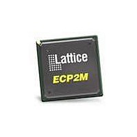
LFE2M20E-5FN256C Lattice, LFE2M20E-5FN256C Datasheet - Page 39

LFE2M20E-5FN256C
Manufacturer Part Number
LFE2M20E-5FN256C
Description
FPGA - Field Programmable Gate Array 19K LUTs 140 I/O SERDES DSP -5
Manufacturer
Lattice
Datasheet
1.LFE2-12SE-6FN256C.pdf
(389 pages)
Specifications of LFE2M20E-5FN256C
Number Of Macrocells
19000
Maximum Operating Frequency
311 MHz
Number Of Programmable I/os
140
Data Ram Size
1246208
Supply Voltage (max)
1.26 V
Maximum Operating Temperature
+ 85 C
Minimum Operating Temperature
0 C
Mounting Style
SMD/SMT
Supply Voltage (min)
1.14 V
Package / Case
FPBGA-256
Lead Free Status / RoHS Status
Lead free / RoHS Compliant
Available stocks
Company
Part Number
Manufacturer
Quantity
Price
Company:
Part Number:
LFE2M20E-5FN256C
Manufacturer:
Lattice Semiconductor Corporation
Quantity:
10 000
- Current page: 39 of 389
- Download datasheet (5Mb)
Lattice Semiconductor
Top Edge
The PICs on the top edge are different from PIOs on the left, right and bottom edges. PIOs on this edge do not
have DDR registers or DQS signals.
The exact DQS pins are shown in a dual function in the Logic Signal Connections table in this data sheet. Addi-
tional detail is provided in the Signal Descriptions table. The DQS signal from the bus is used to strobe the DDR
data from the memory into input register blocks. Interfaces on the left and right edges are designed for DDR mem-
ories that support 16 bits of data, whereas interfaces on the bottom are designed for memories that support 18 bits
of data.
Figure 2-33. DQS Input Routing for the Left and Right Edges of the Device
DQS
PIO A
PIO B
PIO A
PIO B
PIO A
PIO B
PIO A
PIO B
PIO A
PIO B
PIO A
PIO B
PIO A
PIO B
PIO A
PIO B
2-36
sysIO
Buffer
Delay
LatticeECP2/M Family Data Sheet
PADA "T"
PADA "T"
PADA "T"
PADA "T"
PADA "T"
PADA "T"
PADB "C"
PADB "C"
PADA "T"
PADB "C"
PADB "C"
PADB "C"
PADB "C"
PADB "C"
DQS Pin
PADA "T"
PADB "C"
Assigned
LVDS Pair
LVDS Pair
LVDS Pair
LVDS Pair
LVDS Pair
LVDS Pair
LVDS Pair
LVDS Pair
Architecture
Related parts for LFE2M20E-5FN256C
Image
Part Number
Description
Manufacturer
Datasheet
Request
R

Part Number:
Description:
FPGA - Field Programmable Gate Array 19K LUTs 304 I/O SERDES DSP -5
Manufacturer:
Lattice
Datasheet:

Part Number:
Description:
FPGA - Field Programmable Gate Array 19K LUTs 304 I/O SERDES DSP -5
Manufacturer:
Lattice

Part Number:
Description:
FPGA - Field Programmable Gate Array 19K LUTs 304 I/O SERDES DSP -6
Manufacturer:
Lattice
Datasheet:

Part Number:
Description:
FPGA - Field Programmable Gate Array 19K LUTs 140 I/O SERDES DSP -6
Manufacturer:
Lattice
Datasheet:
Part Number:
Description:
FPGA LatticeECP2M Family 19000 Cells 90nm (CMOS) Technology 1.2V 484-Pin FBGA
Manufacturer:
LATTICE SEMICONDUCTOR
Datasheet:
Part Number:
Description:
FPGA LatticeECP2M Family 19000 Cells 90nm (CMOS) Technology 1.2V 256-Pin FBGA
Manufacturer:
LATTICE SEMICONDUCTOR
Datasheet:
Part Number:
Description:
FPGA LatticeECP2M Family 19000 Cells 90nm (CMOS) Technology 1.2V 256-Pin FBGA
Manufacturer:
LATTICE SEMICONDUCTOR
Datasheet:

Part Number:
Description:
IC FPGA 20KLUTS 140I/O 256-BGA
Manufacturer:
Lattice
Datasheet:

Part Number:
Description:
IC FPGA 20KLUTS 140I/O 256-BGA
Manufacturer:
Lattice
Datasheet:

Part Number:
Description:
IC FPGA 20KLUTS 140I/O 256-BGA
Manufacturer:
Lattice
Datasheet:

Part Number:
Description:
IC FPGA 20KLUTS 304I/O 484-BGA
Manufacturer:
Lattice
Datasheet:

Part Number:
Description:
IC FPGA 20KLUTS 140I/O 256-BGA
Manufacturer:
Lattice
Datasheet:

Part Number:
Description:
IC FPGA 20KLUTS 140I/O 256-BGA
Manufacturer:
Lattice
Datasheet:

Part Number:
Description:
IC FPGA 20KLUTS 304I/O 484-BGA
Manufacturer:
Lattice
Datasheet:


