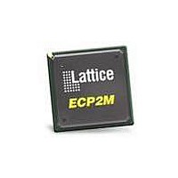
LFE2M20E-5FN256C Lattice, LFE2M20E-5FN256C Datasheet - Page 388

LFE2M20E-5FN256C
Manufacturer Part Number
LFE2M20E-5FN256C
Description
FPGA - Field Programmable Gate Array 19K LUTs 140 I/O SERDES DSP -5
Manufacturer
Lattice
Datasheet
1.LFE2-12SE-6FN256C.pdf
(389 pages)
Specifications of LFE2M20E-5FN256C
Number Of Macrocells
19000
Maximum Operating Frequency
311 MHz
Number Of Programmable I/os
140
Data Ram Size
1246208
Supply Voltage (max)
1.26 V
Maximum Operating Temperature
+ 85 C
Minimum Operating Temperature
0 C
Mounting Style
SMD/SMT
Supply Voltage (min)
1.14 V
Package / Case
FPBGA-256
Lead Free Status / RoHS Status
Lead free / RoHS Compliant
Available stocks
Company
Part Number
Manufacturer
Quantity
Price
Company:
Part Number:
LFE2M20E-5FN256C
Manufacturer:
Lattice Semiconductor Corporation
Quantity:
10 000
- Current page: 388 of 389
- Download datasheet (5Mb)
Lattice Semiconductor
September 2007
November 2009
February 2008
January 2009
August 2007
August 2008
June 2008
April 2008
(cont.)
Date
Version
(cont.)
02.8
02.9
03.0
03.1
03.2
03.3
03.4
03.5
Ordering Information
Pinout Information
Pinout Information
Pinout Information
Pinout Information
Pinout Information
Pinout Information
DC and Switching
DC and Switching
DC and Switching
DC and Switching
DC and Switching
Characteristics
Characteristics
Characteristics
Architecture
Architecture
Architecture
Introduction
Section
(cont.)
sysCLOCK GPLL timing has been updated.
Added ECP2M50 (484/672/900-fpBGA), ECP2M70 (900-fpBGA) and
ECP2M100 (900-fpBGA) pinout information.
1156-fpBGA package option has been removed from the LatticeECP2M
family.
Added Thermal Management text section.
Added LVCMOS33D description.
LatticeECP2M Supply Current has been updated.
Typical Building Block Function Performance, External Switching
Characteristics, Internal Switching Characteristics, Family Timing
Adders, sysCLOCK GPLL Timing, sysCLOCK SPLL Timing, DLL Tim-
ing and sysCONFIG Port Timing Specifications have been updated (tim-
ing rev. A 0.11).
Figure 3-9. Read/Write Mode (Normal) and Figure 3-10. Read/Write
Mode with Input and Output Registers have been updated.
Table 3-8. Channel output Jitter (Max) has been updated.
Signal description has been updated.
Added 1152-fpBGA pinouts for the ECP2M70 and ECP2M100.
Available DDR Interfaces per I/O Bank for the LFE2M35 (484/672-
fpBGA) have been updated.
Family Selection Guide table - Updated number of EBR SRAM Blocks
for the ECP2-70 device.
Removed Read-Before-Write sysMEM EBR mode.
Clarification of the operation of the secondary clock regions.
Removed Read-Before-Write sysMEM EBR mode.
Clarification of the operation of the secondary clock regions.
Added information for [LOC]DQ[num] to Signal Descriptions table.
Updated typical and max. jitter numbers in Channel Output Jitter table
for x10 mode.
Added Channel Output Jitter table for x20 mode.
Updated SPI/SPIm Configuration Waveforms diagram.
Updated footnotes in LatticeECP2 Initialization Supply Current
table.
Updated footnotes in LatticeECP2M Initialization Supply Current
table.
Updated footnotes in SERDES High Speed Data Receiver
(LatticeECP2M Family Only) table.
Updated max. value for t
CONFIG Port Timing Specifications table.
Updated Serial Output Timing and Levels table.
Updated Figure 3-5 MLVDS
Updated Table 3-7 Serial Output Timing and Levels
Updated Table 3-15 Power Down/Power Up Specification
Signal Descriptions table - corrected references to ULM, URM,
LRM (changed to LUM, RUM and RLM), added footnote 5.
7-3
LatticeECP2/M Family Data Sheet
Change Summary
DINIT
parameter in LatticeECP2/M sys-
Revision History
Related parts for LFE2M20E-5FN256C
Image
Part Number
Description
Manufacturer
Datasheet
Request
R

Part Number:
Description:
FPGA - Field Programmable Gate Array 19K LUTs 304 I/O SERDES DSP -5
Manufacturer:
Lattice
Datasheet:

Part Number:
Description:
FPGA - Field Programmable Gate Array 19K LUTs 304 I/O SERDES DSP -5
Manufacturer:
Lattice

Part Number:
Description:
FPGA - Field Programmable Gate Array 19K LUTs 304 I/O SERDES DSP -6
Manufacturer:
Lattice
Datasheet:

Part Number:
Description:
FPGA - Field Programmable Gate Array 19K LUTs 140 I/O SERDES DSP -6
Manufacturer:
Lattice
Datasheet:
Part Number:
Description:
FPGA LatticeECP2M Family 19000 Cells 90nm (CMOS) Technology 1.2V 484-Pin FBGA
Manufacturer:
LATTICE SEMICONDUCTOR
Datasheet:
Part Number:
Description:
FPGA LatticeECP2M Family 19000 Cells 90nm (CMOS) Technology 1.2V 256-Pin FBGA
Manufacturer:
LATTICE SEMICONDUCTOR
Datasheet:
Part Number:
Description:
FPGA LatticeECP2M Family 19000 Cells 90nm (CMOS) Technology 1.2V 256-Pin FBGA
Manufacturer:
LATTICE SEMICONDUCTOR
Datasheet:

Part Number:
Description:
IC FPGA 20KLUTS 140I/O 256-BGA
Manufacturer:
Lattice
Datasheet:

Part Number:
Description:
IC FPGA 20KLUTS 140I/O 256-BGA
Manufacturer:
Lattice
Datasheet:

Part Number:
Description:
IC FPGA 20KLUTS 140I/O 256-BGA
Manufacturer:
Lattice
Datasheet:

Part Number:
Description:
IC FPGA 20KLUTS 304I/O 484-BGA
Manufacturer:
Lattice
Datasheet:

Part Number:
Description:
IC FPGA 20KLUTS 140I/O 256-BGA
Manufacturer:
Lattice
Datasheet:

Part Number:
Description:
IC FPGA 20KLUTS 140I/O 256-BGA
Manufacturer:
Lattice
Datasheet:

Part Number:
Description:
IC FPGA 20KLUTS 304I/O 484-BGA
Manufacturer:
Lattice
Datasheet:


